
Thermal path
Define heat density, operating environment, thermal cycling and the external heat-sink or package interface before selecting Alumina, AlN, ZTA or Si3N4.
EBest PCBA manufactures ceramic PCBs using Alumina, AlN, ZTA and Si3N4 substrates with DPC, DBC, AMB, Thick Film, LTCC and HTCC processes. Material, conductor design, geometry, surface finish and inspection requirements are reviewed based on the released project files.
Initial response within 12 hours. Final material, manufacturing process, test plan and production schedule are confirmed after project file review.
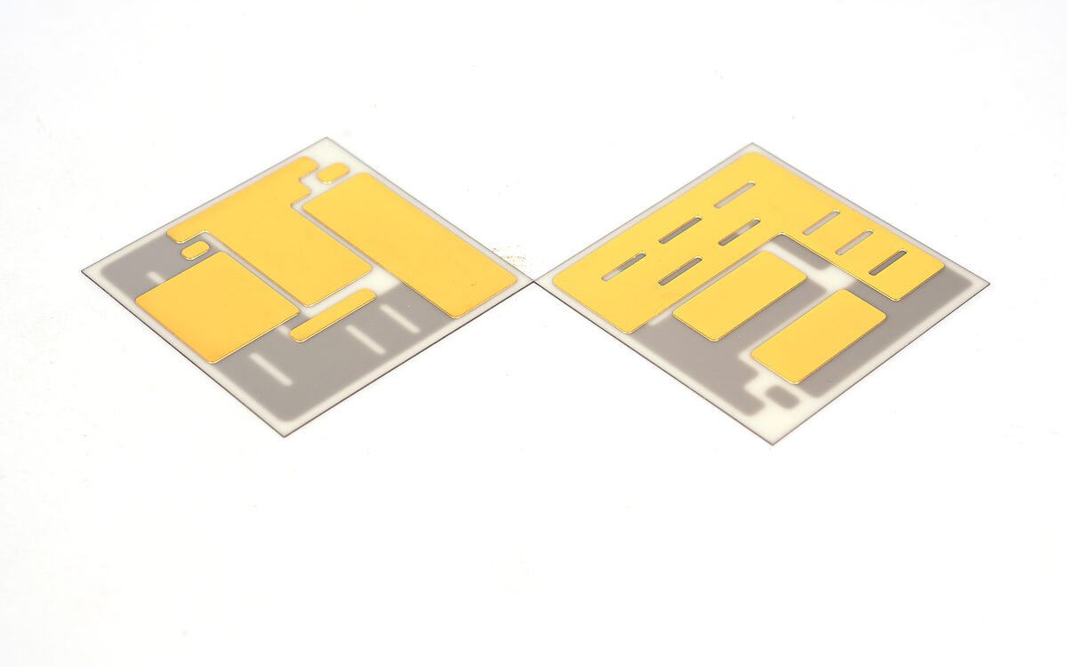
The correct ceramic PCB process depends on the substrate, conductor system, thermal requirements, circuit geometry and assembly interface. These factors should be reviewed together before the manufacturing process is confirmed.
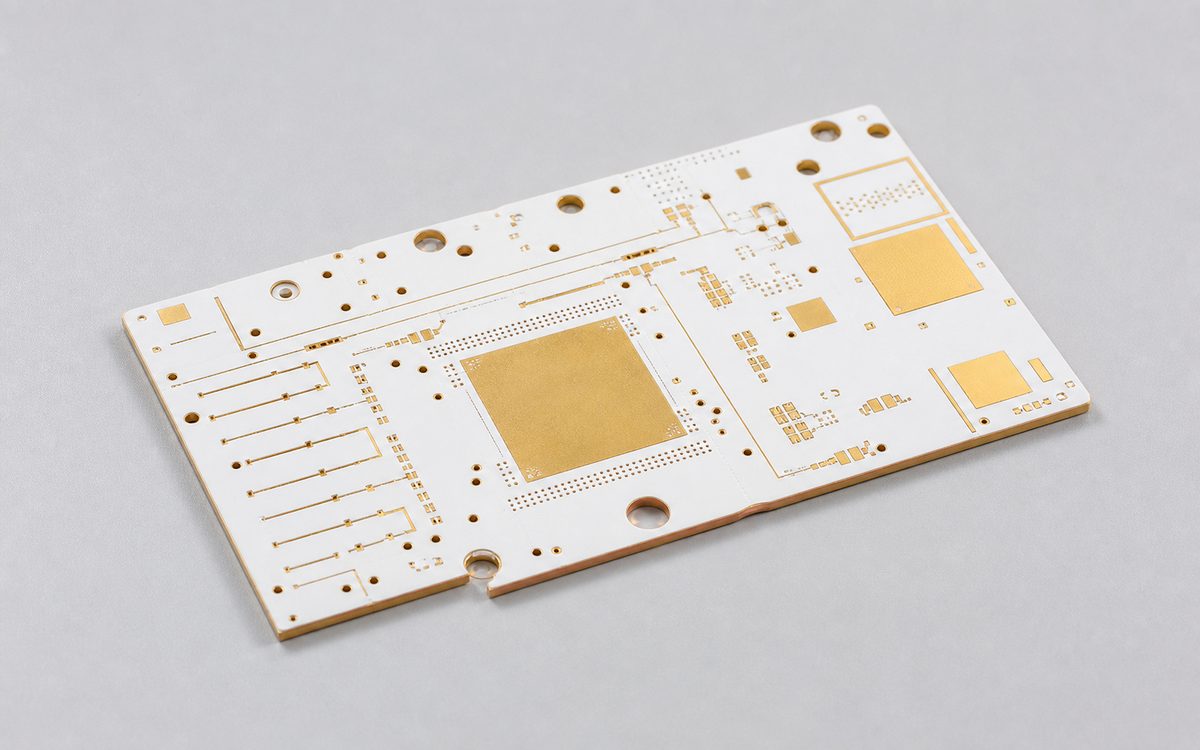
Define heat density, operating environment, thermal cycling and the external heat-sink or package interface before selecting Alumina, AlN, ZTA or Si3N4.
Confirm voltage withstand, creepage, dielectric behavior and conductor-to-edge requirements together with substrate thickness and surface condition.
Fine patterned copper, thick copper, printed conductor paste and co-fired metallization follow different DPC, DBC, AMB, Thick Film, LTCC or HTCC routes.
Soldering, wire bonding, die attach, component clearance, finish, flatness and inspection requirements must be defined before the board route is released.
Use the following process options as an initial reference. Final material, copper thickness, geometry, surface finish, tolerance and production schedule are confirmed after project review.
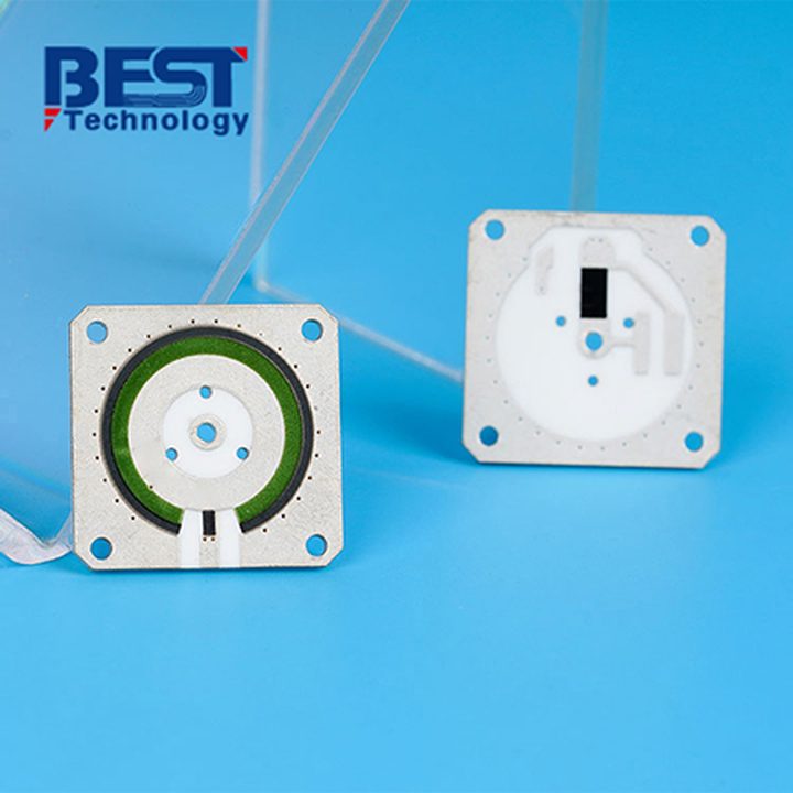
For printed paste circuits where firing profile, glaze, conductor geometry and downstream bonding or soldering must be aligned.
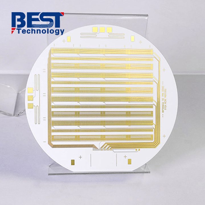
For finer copper geometry where conductor thickness, adhesion, surface finish and thermal interface are reviewed as one build.
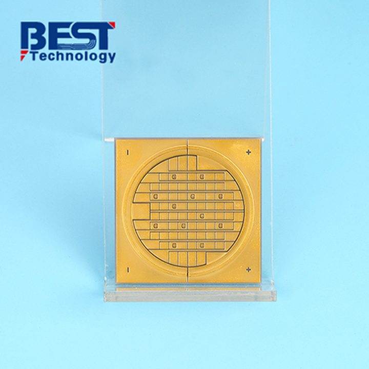
For higher-current power circuits where bonded copper, ceramic isolation, thermal cycling and module attachment control the route.
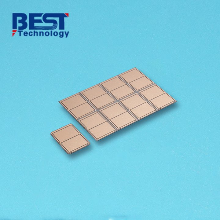
For power-module builds where higher current, cycling load, substrate selection and bonding reliability must be confirmed together.
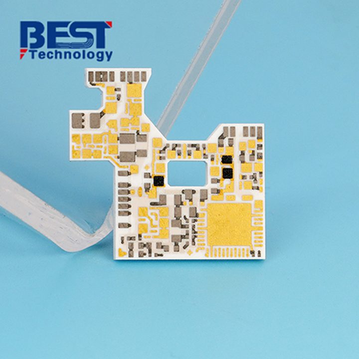
For multilayer ceramic circuits where conductor compatibility, cavities, buried structures and shrinkage control affect release.
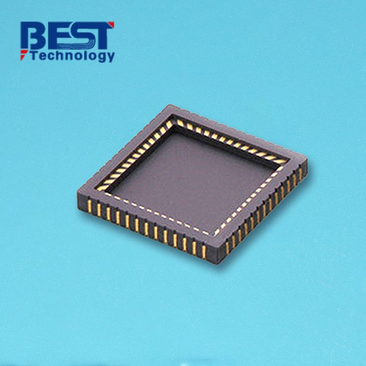
For ceramic packages where conductor system, firing route, multilayer structure and environmental reliability define the build.
The values below are general capability references. Final manufacturability, tolerances and process combinations are confirmed after reviewing the actual project files.
| Capability Item | Standard Capability | Engineering Review Required |
|---|---|---|
| Ceramic substrates | Al2O3, AlN, ZTA and Si3N4 | Glass, quartz, sapphire and special Alumina grades require project confirmation. |
| Process routes | DPC, DBC, AMB, Thick Film, LTCC and HTCC | Layer count, conductor system and route-specific structures are reviewed together. |
| Layer reference | DPC/DBC/AMB: single or double sided. LTCC/HTCC: 1–2, 4 or 6 layers. Thick Film: route-specific construction. | LTCC 6–14 layers and conflicting or special multilayer combinations require engineering evaluation. |
| Outer copper | DPC: 0.5–3 oz. DBC/AMB: 3–12 oz. | Final copper, ceramic, line geometry and bonding combination follow design review. |
| Maximum dimension | 130 × 180 mm screening reference | Larger size and Thick Film format are reviewed by process and panel method. |
| Substrate thickness | Al2O3/AlN: 0.38, 0.635 and 1.0 mm. Si3N4: 0.25 and 0.32 mm. | Thicker and non-standard substrate combinations require availability and process evaluation. |
| Line width / spacing | 0.10 / 0.10 mm general screening reference; copper-dependent rules apply. | Down to 0.076 / 0.076 mm is evaluation-required and route-specific. |
| Surface finish | OSP, ENIG, immersion silver, immersion tin, ENEPIG and hard gold can be reviewed. | Finish must match soldering, wire bonding, conductor system and storage requirements. |
| Finished thickness | 0.2–2.0 mm screening reference | 2.0 mm and above requires project evaluation. |
Important: published values are quotation-screening references. Final manufacturability, tolerances, inspection plan, production route and schedule are released only after engineering review of the project files.
Ceramic PCB processes vary by substrate and conductor system. EBest PCBA first confirms the appropriate process, then aligns manufacturing controls and inspection requirements with the approved construction.
Gerber or ODB++, drawing, material, conductor, quantity, thermal and assembly notes are checked for missing inputs.
Substrate, thickness, conductor system and DPC, DBC, AMB, Thick Film, LTCC or HTCC route are confirmed before pricing.
Printing, plating, bonded copper or co-fired operations follow the approved construction, geometry, holes, outline and finish.
Dimensions, conductor geometry, isolation, surface condition, traceability and assembly handoff are checked before shipment.
Inspection requirements should match the ceramic substrate, conductor system, circuit structure and downstream assembly method.
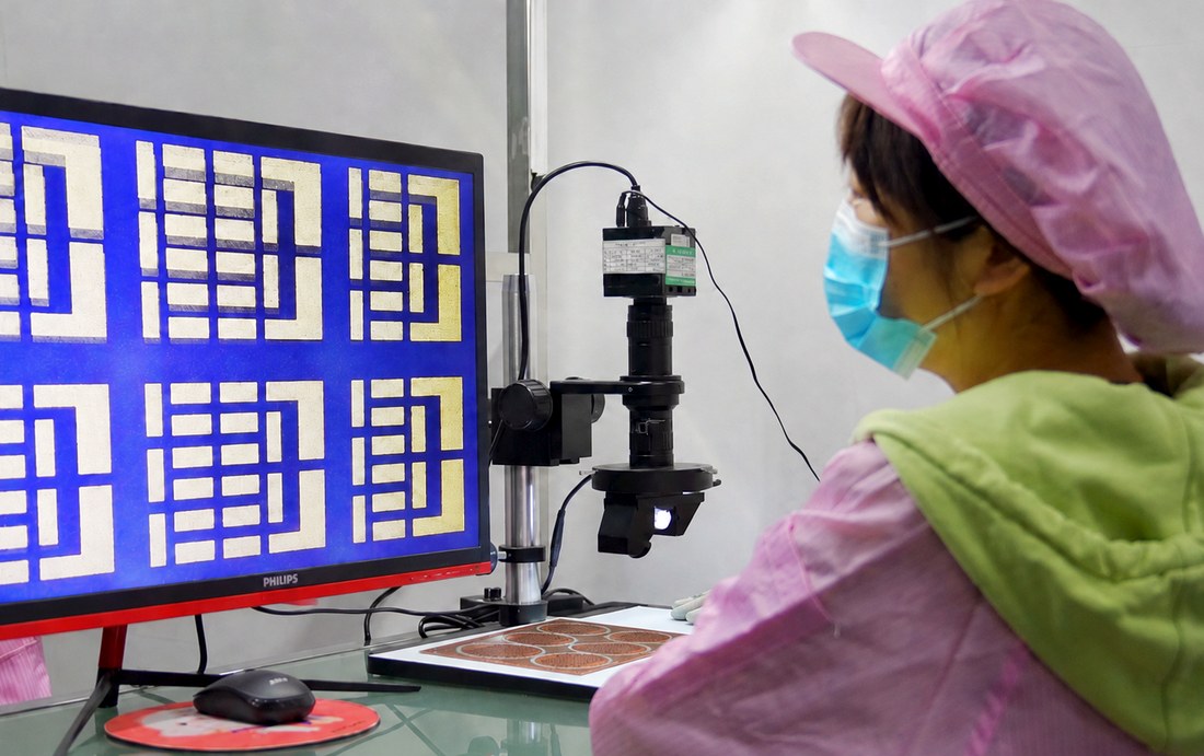
Material identification, thickness, surface condition and project-specific mechanical requirements are checked before circuit processing.
Line width, spacing, conductor or copper thickness, pads, holes, outline and edge clearance follow the released drawing and route.
Glaze, solder mask, finish, via or through-hole strategy, wire-bonding and soldering interfaces are checked for compatibility.
Continuity, isolation and project-defined inspection or reliability requirements are confirmed in the quotation and quality plan.
Released revision, lot information, inspection records and packaging route are aligned with the order and downstream assembly needs.
Ceramic PCBs are commonly used in applications that require efficient heat dissipation, electrical isolation, dimensional stability and reliable performance in demanding environments.

Review isolation, stability, documentation, inspection and assembly requirements for diagnostic and treatment equipment.
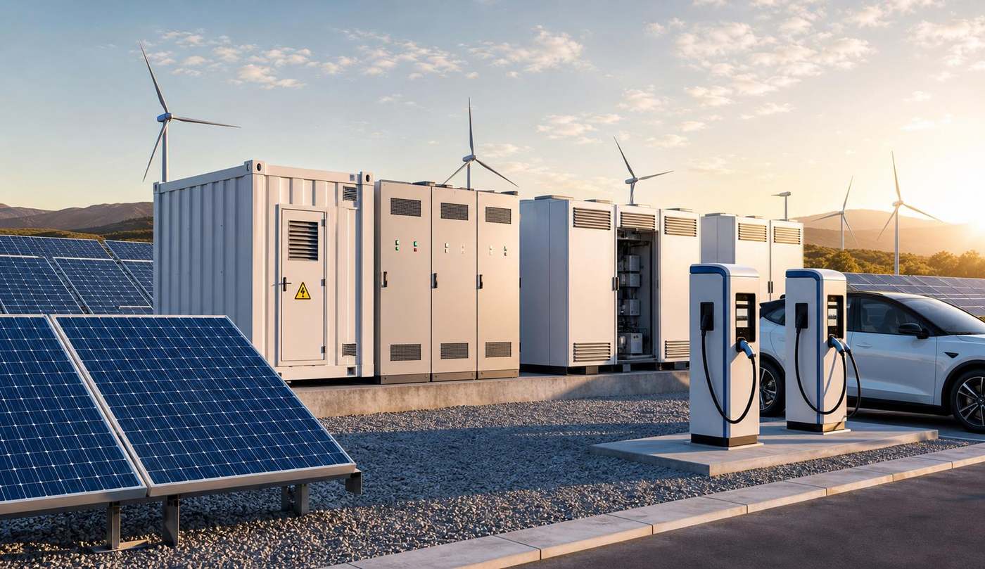
Assess heat flow, current, copper construction, thermal cycling and power-module interfaces.

Connect thermal and mechanical requirements to substrate, copper, attachment and traceability decisions.
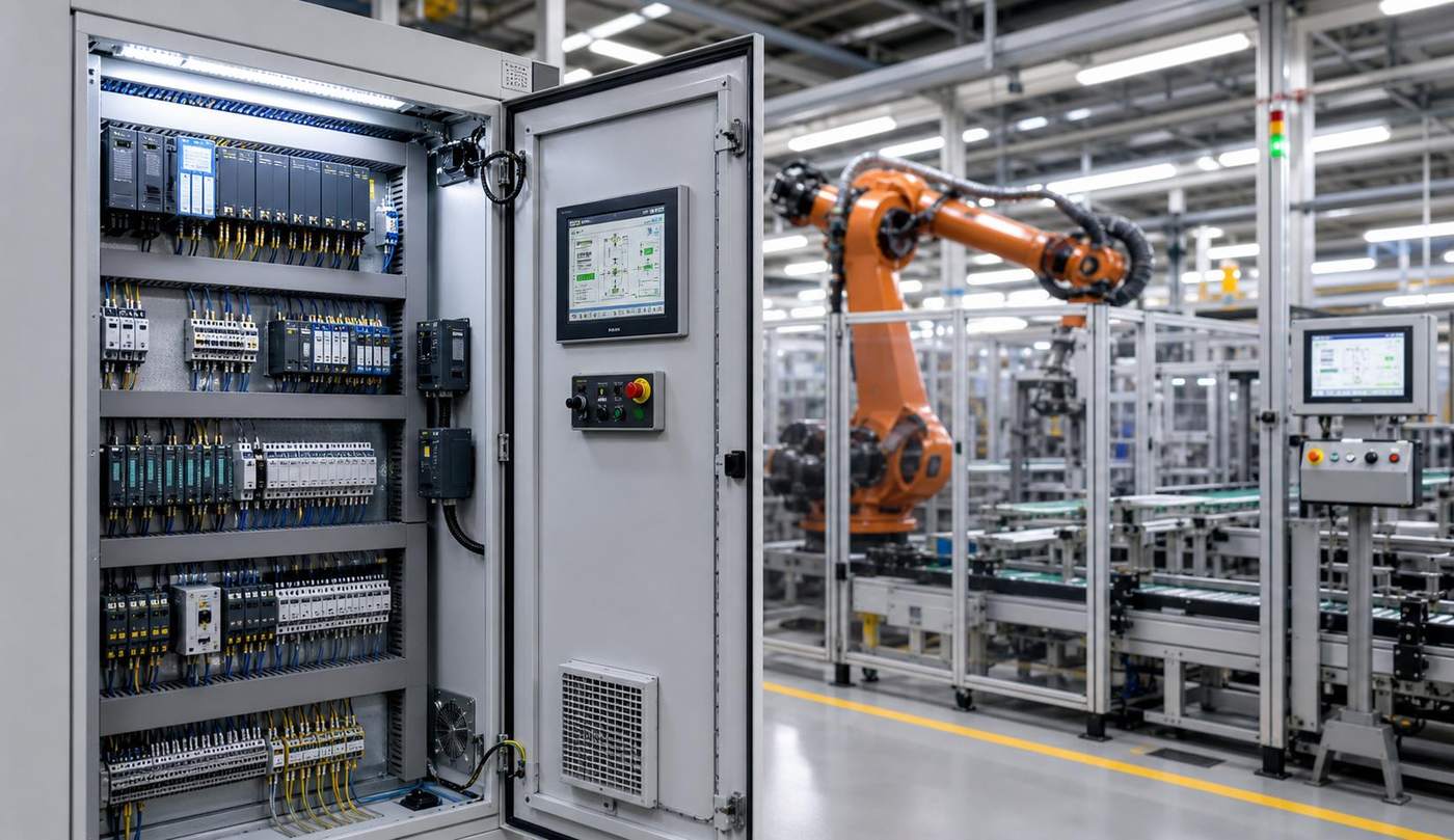
Review power density, insulation, operating environment, repeatability and downstream assembly needs.
You can send the available files even if some details are still open. EBest PCBA will identify any missing information required before the quotation is finalized.
Send your available board data, application requirements and open questions. EBest PCBA will review the substrate, manufacturing process, conductor system, geometry, surface finish and assembly requirements before quotation.
These FAQs cover common questions about ceramic PCB materials, manufacturing processes, surface finishes, quotations and assembly.