
Rigid islands in one build
Connect component areas without using separate PCBs and cables for each section.
Combine rigid component areas and flexible interconnects in a single PCB. EBest PCBA reviews the stack-up, transition geometry, bend requirements, HDI features, impedance requirements, and assembly needs before quotation.
Response within 12 hours · Final manufacturing requirements, test plan, and delivery schedule confirmed after file review
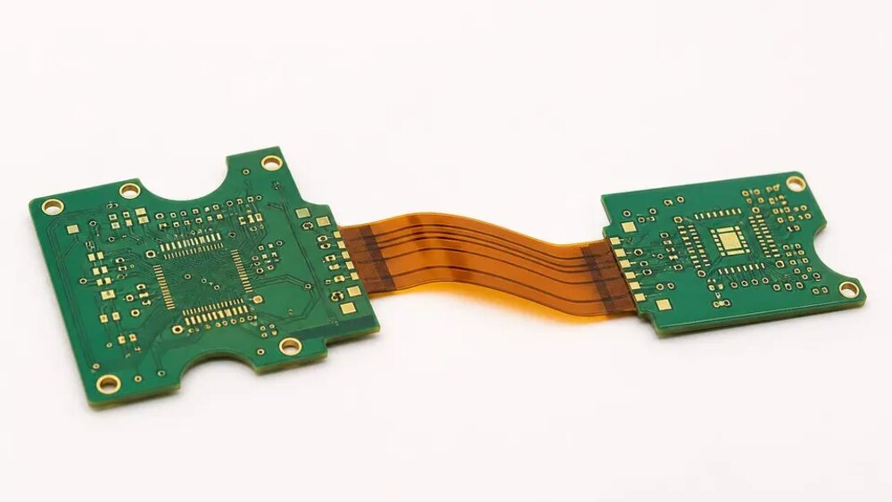
Rigid-flex PCBs are useful when separate boards, cables, or connectors take up too much space or add assembly complexity. The rigid and flex sections should be reviewed together before fabrication.
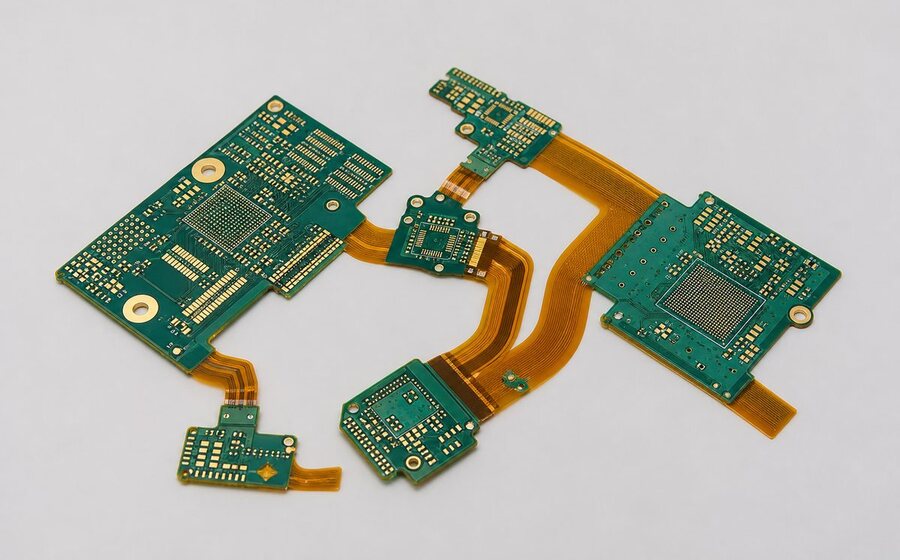
Connect component areas without using separate PCBs and cables for each section.
Confirm bend radius, fold direction, trace direction, and mechanical keep-outs before fabrication.
Replace selected cables and connectors with integrated flex interconnects where the product design allows.
Review carriers, connectors, component keep-outs, and flex handling before PCBA assembly.
Final capability depends on the complete combination of layer count, flex-layer position, copper, transition geometry, materials, surface finish, impedance, and assembly handling
| Capability item | Standard Range | Special Review |
|---|---|---|
| Layer count | 2–10 layers for supported rigid-flex constructions | 11–20 layers; stack-up, registration, via structure, and materials must be confirmed from the project files |
| Flex-layer position | Outer-layer or middle-layer flex constructions | Final position follows assembly, bend, copper and lamination requirements |
| Finished thickness | 0.3-3.0 mm | Tolerance and handling requirements are confirmed from the final stack-up. |
| Minimum flex width | 2.0 mm | Narrow or mechanically constrained regions require strain and process review |
| Inner line / space | 3 / 3 mil at 18 um finished copper reference | Finer geometry or different copper thicknesses require additional manufacturability review. |
| HDI structure | 1+n+1 reference | Higher-order HDI, special via combinations and any-layer structures require review |
| Impedance | ±10% reference | Rigid and flex stack-ups, test coupons, and measurement methods are confirmed for each project. |
| Surface finish | ENIG, plated gold, OSP and tin routes | ENEPIG and connector-specific plating require feature and material assessment |
Rigid-flex construction should be selected based on how the product will be installed, folded, assembled, and tested. More complex structures may need additional engineering review.
A direct architecture for connecting separated mounting areas through a defined folding or routing path.
Integrates several functional zones where component density and enclosure geometry require distributed rigid areas.
Flex-layer position is selected based on protection, assembly access, copper geometry, and lamination requirements.
Microvia and build-up options are evaluated with registration, resin, copper and transition-zone constraints.

Material selection affects thickness, registration, resin flow, bend performance, and dimensional stability. The quotation should identify the actual material system instead of only stating ‘FR4 plus flex.’
FR4 and selected special rigid materials are reviewed against thermal, electrical and thickness requirements.
Adhesive or adhesiveless polyimide cores and copper options are selected for the flexible regions.
Low-flow prepreg or adhesive must limit resin movement around rigid-flex transitions and openings.
Coverlay, PI support, local reinforcement and pressure-sensitive adhesive are coordinated with assembly.
The transition zone carries mechanical strain between rigid and flexible materials. Routing, holes, resin flow, coverlay, and geometry should be checked before fabrication.
A useful DFM review should identify the affected zone, design rule, risk, and required change instead of only returning a general manufacturability result.
Confirms rigid, flexible and adhesive layers, copper weights, coverlay and overall thickness.
Reviews conductor clearance, resin flow, support, openings and corner radii at the boundary.
Check PTH, buried vias, and laser vias against the transition zone, copper construction, and HDI requirements.
Examines trace direction, width changes, bend area, fold orientation and mechanical constraints.
Coordinates trace geometry and dielectric behavior across rigid and flexible stack sections.
Plans tooling, carriers, component keep-outs, connector support and flex handling during PCBA.
The exact process depends on the layer build and HDI structure. Material approval, transition-zone control, lamination, and testing are based on the approved project data.
Confirm stack, zones, bends, tolerances and open questions.
Confirm rigid laminate, polyimide, copper, coverlay, and bonding materials.
Image and etch the rigid and flex conductors according to the approved artwork.
Control layer registration, resin flow, transition openings, and hole locations.
Complete plating, solder mask, coverlay and final outline.
Apply dimensional, visual and electrical checks to the agreed plan.
These examples show typical rigid-flex structures and the information that needs to be confirmed before quotation.
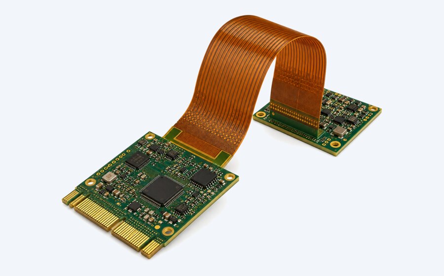
Two rigid mounting areas connected by a defined flex zone for enclosure routing or controlled installation.
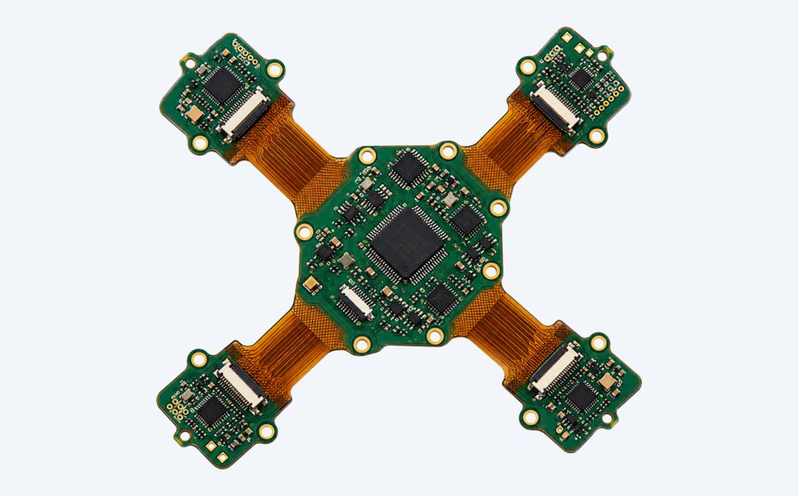
Several rigid functions connected through flexible routing where stack, registration and HDI decisions are tightly linked.
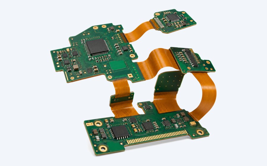
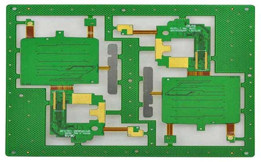
A repeated rigid-flex layout that requires panel support, tooling, and PCBA handling to be planned together.
Partial files can start the review. A complete package helps confirm the stack-up, manufacturing requirements, and quotation faster.
Send the stack-up, rigid/flex zone drawing, and mechanical requirements. EBest PCBA will review the manufacturing requirements and confirm the details before quotation.