
Skip to content
Home / Services / PCB Design
PCB layout and production-file engineering

PCB Design Services From Schematic to Production-Ready Files

Send your available schematic, BOM, board outline and design requirements. EBest PCBA provides PCB layout, stack-up and impedance planning, DFM/DFA review and production-file preparation for the intended PCB fabrication and PCBA assembly route.

4 Core ServicesLayout through release4 PCB TypesFR4, FPC, ceramic, MCPCB5–10 DaysTypical layout projects12h ResponseInitial project check
Engineering review before layout releasePCB DESIGN
EBest PCBA engineers reviewing PCB design files
Project fit, missing inputs, design scope and schedule are confirmed before work begins.
Core PCB design services

Four Services Required to Move a Design Into Production

The quotation states whether the work includes component placement, routing, stack-up and impedance design, DFM/DFA review, and preparation of Gerber, drill, centroid and assembly files.

01

PCB Layout Design

Component placement and routing based on your schematic, BOM, board outline and confirmed design requirements.

02

Stack-up & Impedance Design

Layer construction and impedance requirements coordinated with the intended PCB manufacturing process.

03

DFM & DFA Review

PCB fabrication and PCBA assembly risks reviewed before the production files are released.

04

Production File Preparation

Agreed design, fabrication and assembly files organized for quotation, prototype and production.

Common PCB types

PCB Types We Design

Choose the material platform closest to your product. EBest reviews the schematic, component density, mechanical limits, thermal requirements and manufacturing process before confirming the design schedule.

Typical PCB layout projects take 5–10 working days. Complex structures, special materials and additional review rounds are scheduled after file review.
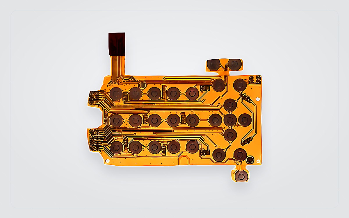
Flexible PCB FPC design example

Flexible PCB (FPC)

Flexible interconnect layouts with bend areas, stiffeners, connector interfaces and space limits considered.
Design scheduleConfirmed after file review
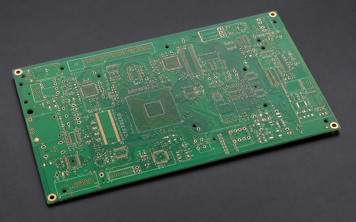
FR4 PCB design example

FR4 PCB

Single-layer, double-sided and multilayer layouts for industrial, control and general electronic products.
Design scheduleConfirmed after file review
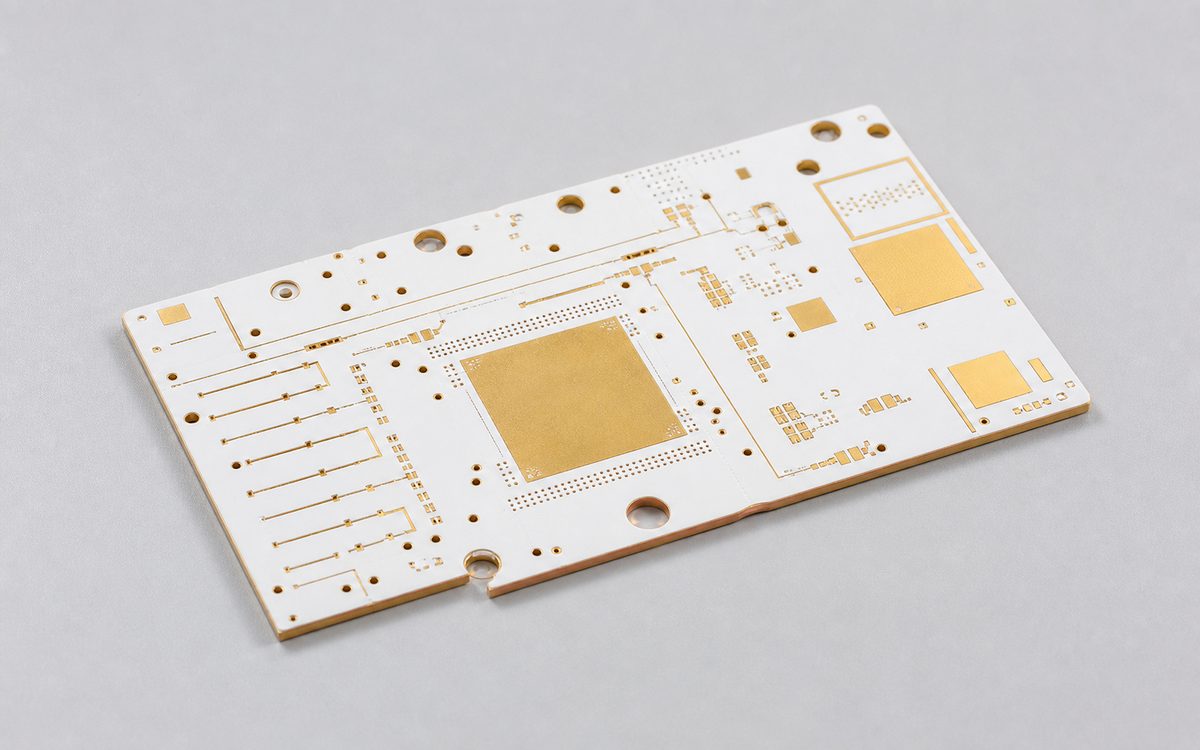
Ceramic PCB design example

Ceramic PCB

Layouts for thermal, power and high-reliability applications using ceramic substrate requirements.
Design scheduleConfirmed after file review
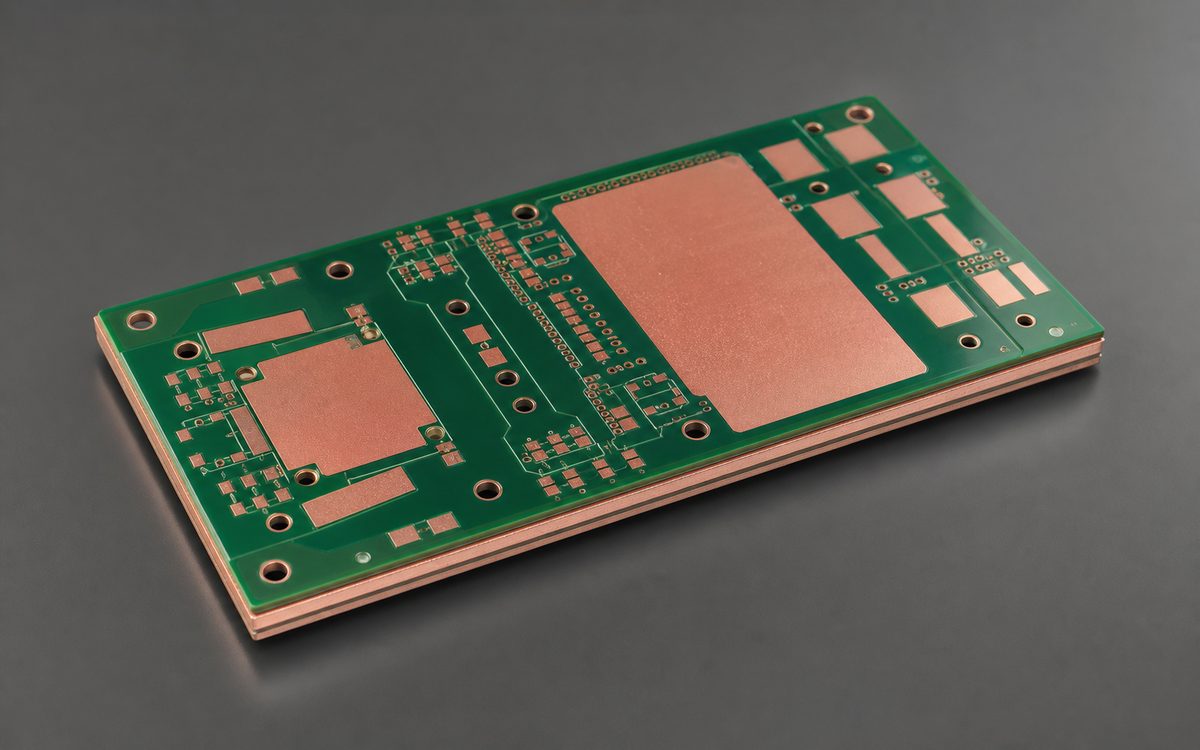
Metal core PCB MCPCB design example

Metal Core PCB (MCPCB)

Thermal-focused layouts for LED, power conversion and other heat-sensitive electronic products.

Design scheduleConfirmed after file review
Documented project evidence

Verified PCB Layout Project Examples

These PCB layout projects and technical details are documented in the EBest company profile. No unverified cycle, yield or cost-saving claims are added.
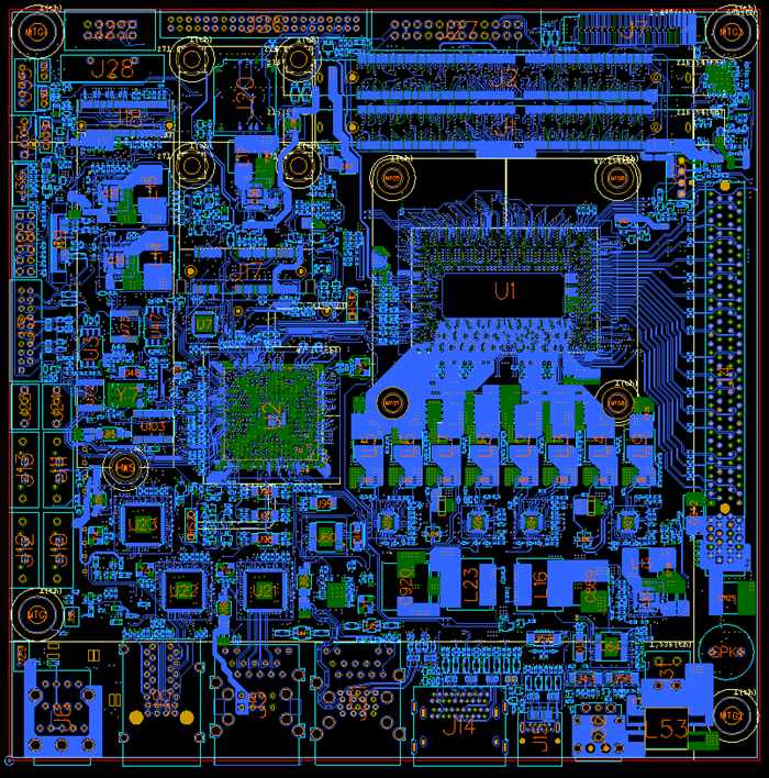
mITX industrial control motherboard PCB layout

mITX Industrial-Control Motherboard

Compact industrial motherboard layout supporting multiple processor options and production interfaces.
Documented platform: Intel Xeon E3, Core i7/i5 or Celeron G3900EDocumented interfaces: 2× DDR4 SODIMM, 4× SATA Gen 3, PCIe x16 Gen 3 and USB 3.0/2.0Evidence status: Published as a PCB design case in the company profile
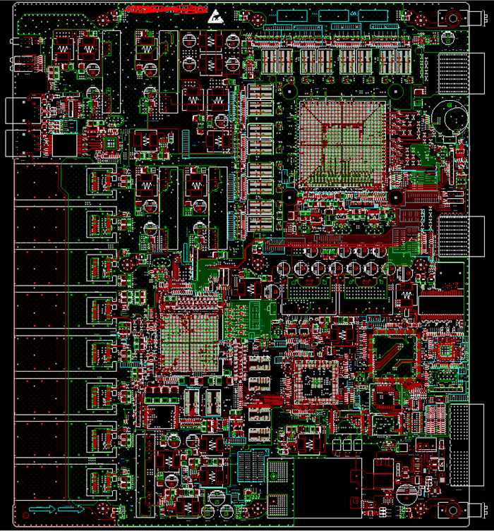
ATCA network switching motherboard PCB layout

ATCA Network-Switching Motherboard

High-density network-board layout documented around switching, memory and high-current requirements.
Documented platform: Broadcom chipset architectureDocumented requirements: Up to 60A, 8× 10G optical networks and 8 DDR3 groupsEvidence status: Published as a PCB design case in the company profile
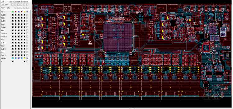
32-port 100G QSFP28 convergence splitter PCB layout

32×100G QSFP28 Convergence Splitter

High-speed multilayer layout example for dense optical-network connectivity and controlled differential routing.

Documented platform: Marvell 98CX8522Documented requirements: 25G differential-pair rate and 16-layer boardEvidence status: Published as a PCB design case in the company profile
Have a similar PCB design project?Start with your available requirements; confidential files are optional for the first discussion.
Discuss Your PCB Design Requirements
Inputs and deliverables

What You Provide and What You Receive

You do not need every file before contacting us. Start with the information currently available; our first review identifies what is still required.

You Provide

  • Schematic or netlist
  • BOM and critical component information
  • Board outline or mechanical drawing
  • Connector, interface and critical routing requirements
  • Target completion date and production plan
File upload is optional for the first project check. Request an NDA before sharing confidential design data when required.

You Receive

  • PCB design source files as agreed
  • Gerber or ODB++ and NC drill files
  • Fabrication and assembly drawings
  • Pick-and-place data
  • Agreed 3D, library and release files
The quotation confirms the design scope, review stages, deliverables, lead time and revision conditions before work begins.
Engineering trust

Design Decisions Reviewed for Real Manufacturing

The objective is not only to finish the layout. PCB layout, DFM and manufacturing reviews connect the released design to the intended fabrication and assembly process.

EBest PCBA PCB layout engineer reviewing a board design before manufacturing
Representative PCB layout and manufacturability review before file release.

PCB Layout Engineer

Owns placement, routing and the confirmed electrical and mechanical layout requirements.

Manufacturing Engineer

Checks that the released construction and file package align with the intended PCB and PCBA route.

Meet the engineering approach

Controlled File Release

Design revisions, review comments and released files are controlled against the approved project baseline.

Project route

Four Steps From Project Check to File Release

01

Check Project Fit

Share the PCB type, available files, target date and a short description. Confidential files are not required at this stage.

02

Confirm Scope & Lead Time

EBest identifies missing inputs and confirms the service scope, deliverables, schedule and quotation process.

03

Design & Review

PCB layout proceeds through the agreed review points, with comments and revisions tracked against the project baseline.

04

Release Agreed Files

The approved source, fabrication and assembly files are organized and released according to the quotation.

How quotations are prepared

Board type, layer count, component density, routing complexity, review requirements and required deliverables determine the design quotation.

Scope boundary

Standard PCB layout service covers the agreed board-design files. Electrical circuit design, firmware and product certification can be quoted separately when required.

Ready to Turn Your Schematic Into Production-Ready PCB Files?

Share your schematic, board outline, BOM or current design files. EBest PCBA will review the available information, identify missing inputs, and confirm the design scope, deliverables and schedule before work begins.

Initial response within 12 hours. Incomplete files are accepted for the first project review.
FAQ

PCB Design Questions Before Starting

Can I ask for a project check without sending confidential files?
Yes. Start with the PCB type, current project stage, target date and a short description. File upload is optional for the first project check, and an NDA can be requested before confidential files are exchanged.
What information is needed to start PCB design?
Provide the schematic or netlist, BOM, board outline or mechanical drawing and known interface, routing, impedance or production requirements. If information is missing, the first review will identify what is still required.
How long does PCB design take?
Typical PCB layout projects take 5–10 working days. FR4, flexible, ceramic and metal-core designs may require different review depth, so final timing is confirmed after the input files, structure, materials, review stages and deliverables are checked.
How is the PCB design quotation calculated?
The quotation considers board type, layer count, component density, routing complexity, review requirements, required deliverables and the agreed revision process.
What files will I receive?
The quotation defines the release package. It may include native PCB source, Gerber or ODB++, NC drill files, fabrication and assembly drawings, pick-and-place data and agreed 3D or library files.
How are design changes and revisions controlled?
Review points and the project baseline are confirmed before work begins. Requested changes are checked against that baseline, and any effect on scope, cost or schedule is clarified before implementation.
Can the design continue into PCB manufacturing and PCBA assembly?
Yes. When required, the released design can continue into PCB fabrication, component sourcing, PCBA assembly, inspection and testing through the agreed manufacturing process.