
Fine-Pitch BGA Escape
Use microvias and finer geometry when through-hole fan-out consumes routing channels or blocks power and ground access.
High-density interconnect manufacturing
Review laser microvias, blind and buried vias, fine-line routing, and via-in-pad requirements before quotation. EBest PCBA reviews the stack-up, drill sequence, copper geometry, and assembly requirements based on the project files.
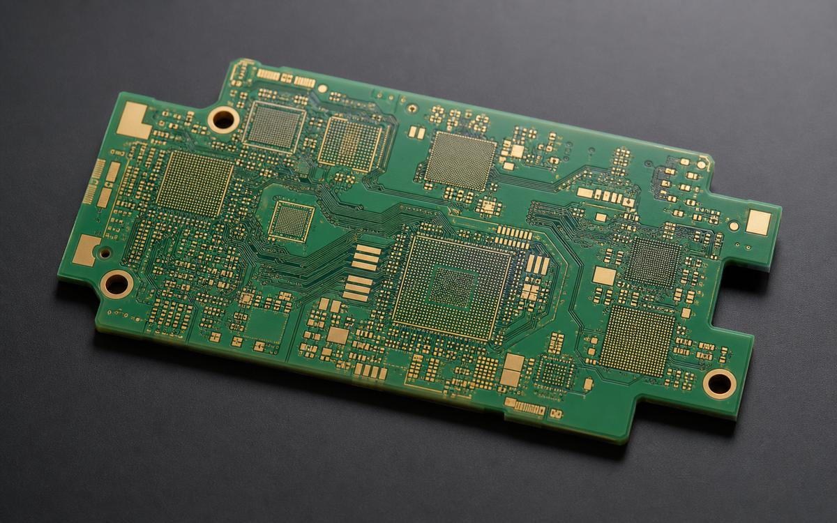
Start with the design constraint
HDI affects the stack-up, drilling sequence, registration, copper balance, and cost, so it should be considered before the layout is finalized.
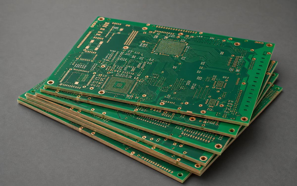
Use microvias and finer geometry when through-hole fan-out consumes routing channels or blocks power and ground access.
Reduce board area while balancing layer count, dielectric thickness, routing density, and reliability.
Move selected connections between layers while controlling drill depth, target land, plating and sequential lamination requirements.
Review fill, planarization, cap plating, pad size, and assembly requirements before approving the VIPPO structure for fabrication.
Construction selection
Each additional build-up cycle adds process time and tighter registration requirements. EBest PCBA confirms the required structure from the layer connectivity, via map, and approved stack-up.
Required layer transitions determine the number of laser-drilling and lamination cycles. Cost and lead time depend on the final build-up structure.
Standard structures and items requiring additional review are identified before quotation.One build-up layer on each side of the core structure for first-level microvia access and controlled BGA escape.
Two build-up layers per side when routing requires additional blind-via transitions.
Layer-to-layer microvia interconnect reviewed against registration, reliability and the complete via map.
Fill, planarization and cap plating reviewed with pad size, finish and assembly expectations.
HDI Capability Review From Your Production Files
The values below are general manufacturing references. Final capability depends on copper weight, plating, hole depth, dielectric thickness, and registration, so the design files must be reviewed before quotation.
| Review Item | General Reference | Special Review | Decision Factors |
|---|---|---|---|
| Laser microvia | 0.10 mm general reference | Structure-specific review | Dielectric depth, aspect ratio, capture pad, fill and plating |
| Finished mechanical hole | 0.20 mm minimum reference | 0.15 mm requires special review | Board thickness, aspect ratio, plating and tolerance |
| Inner line width / spacing | 4 / 4 mil at 0.5-1 oz copper | 3 / 3 mil requires special review | Base copper, finished copper, etching compensation and yield |
| Through-hole aspect ratio | Up to 8:1 reference | Up to 10:1 requires special review | Hole diameter, board thickness and plating distribution |
| FR-4 layer count | 1-10 layer reference | 10-32 layers reviewed as special | HDI cycles, material system, copper balance and registration |
| Build-up structure | 1+N+1 after stack-up review | 2+N+2, stacked/staggered, and Any-Layer require project review | Connectivity, drill sequence, lamination cycles and reliability target |
| Surface finish | OSP, HASL, ENIG, immersion silver or tin | ENEPIG and hard-gold combinations by review | Fine-pitch assembly, wire bonding, storage and contact life |
| Impedance control | Target and tolerance confirmed from the approved stack-up and coupon requirements | Material Dk, dielectric thickness, copper geometry and finished copper | |
Line width / spacing means two different dimensions: the first value is the minimum copper trace width; the second is the minimum clearance between adjacent traces. Final manufacturability and schedule are confirmed from project files.
HDI Manufacturing Process
The exact process depends on the approved build-up, materials, and inspection plan. Each lamination and drilling cycle is checked against the approved stack-up and via structure.
Check layer connectivity, microvia depth, target lands, copper and impedance requirements.
Control dielectric, laser depth, target lands and registration for each build-up cycle.
Check via-wall plating, copper build, resin fill, planarization, and cap plating when required.
Protect fine geometry, copper balance and impedance-critical routing through production.
Confirm ENIG, OSP or project-specific finish against BGA, via-in-pad and soldering needs.
Complete electrical, dimensional, microsection, and other required inspections before shipment.
Engineering and inspection evidence
HDI issues often occur around capture pads, microvia plating, registration, resin fill, fine-line copper, and assembly pads. Inspection should focus on these areas before shipment. 直接删除
Review missing inputs, drill definitions, via-to-pad geometry, copper weight and the build sequence before quotation.
Confirm target-land access, annular relationships and layer alignment through the sequential build-up.
Use microsections when required to check plating, fill, interfaces, and finished hole structure.
Perform electrical testing and impedance verification against the approved data and coupon plan.
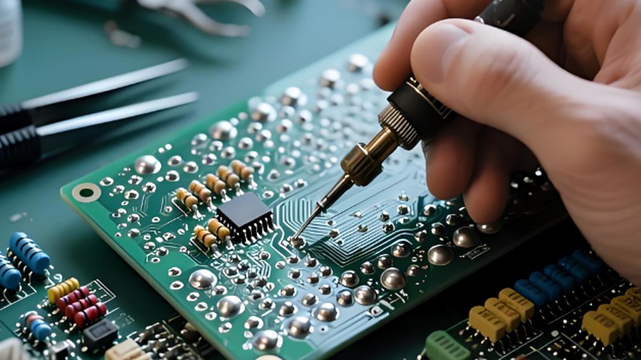
Anonymized engineering case profiles
These examples show how typical HDI requirements are reviewed before fabrication. Final stack-up, via structure, and inspection requirements depend on the actual project files.
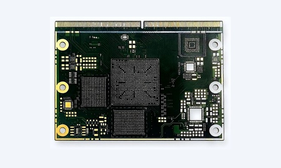
A compact processor board used microvias to create additional BGA escape channels while maintaining the required stack-up, copper, and impedance.
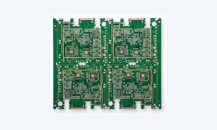
Fine-pitch routing and high-speed interfaces had to be reviewed against the actual reference planes, dielectric data and layer transitions.
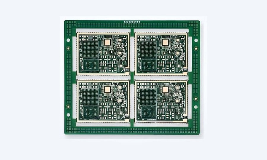
Dense digital routing shared the board with power and I/O areas, so material selection, fine-line geometry, and the build sequence were reviewed together before fabrication.
Industry applications

Network processors, RF modules and compact routing with impedance review.

Portable diagnostic and monitoring products with strict documentation and reliability requirements.

Compact sensing and control modules reviewed for thermal and vibration conditions.

Embedded controllers and communication boards where compact size and reliable operation are required.
Prepare a quote-ready review
Send the files you have. EBest PCBA will review the stack-up, microvia, copper, impedance, and assembly requirements before quotation and production.