
PCB Manufacturing
FR4 multilayer, flexible, rigid-flex, metal-core, ceramic and HDI boards manufactured to approved files and construction requirements.
Explore PCB Fabrication →From PCB fabrication and component sourcing to SMT/THT assembly, functional testing and box build, EBest PCBA supports prototypes, pilot runs and volume production with dedicated engineering support.
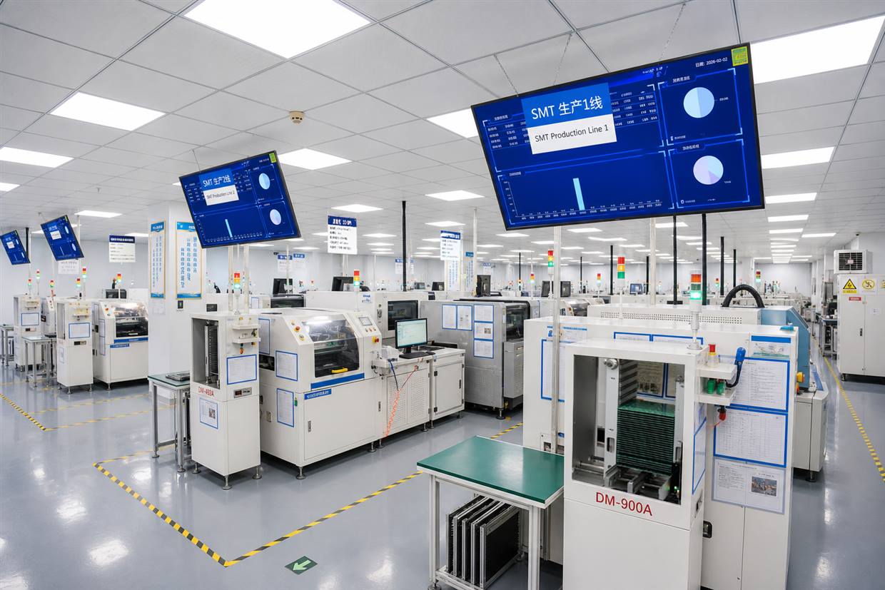
Choose bare-board fabrication, assembled boards or finished-product integration. Component sourcing, inspection and testing are defined around your project requirements.
FR4 multilayer, flexible, rigid-flex, metal-core, ceramic and HDI boards manufactured to approved files and construction requirements.
Explore PCB Fabrication →Coordinate BOM review, component sourcing, SMT/THT assembly, inspection and project-defined electrical or functional testing.
Explore PCBA Assembly →Integrate PCBAs, enclosures, cables and specified parts, with assembly checks, testing and packaging agreed for your product.
Explore Box Build →Explore our PCB manufacturing facilities, SMT assembly equipment, inspection systems and production traceability capabilities.
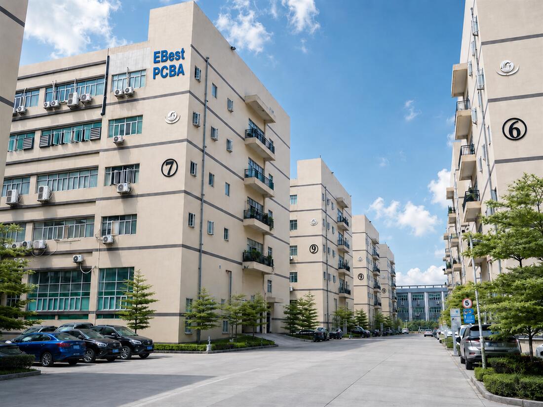
Coordinate PCB fabrication, component sourcing, assembly and testing through manufacturing operations in China and Vietnam.
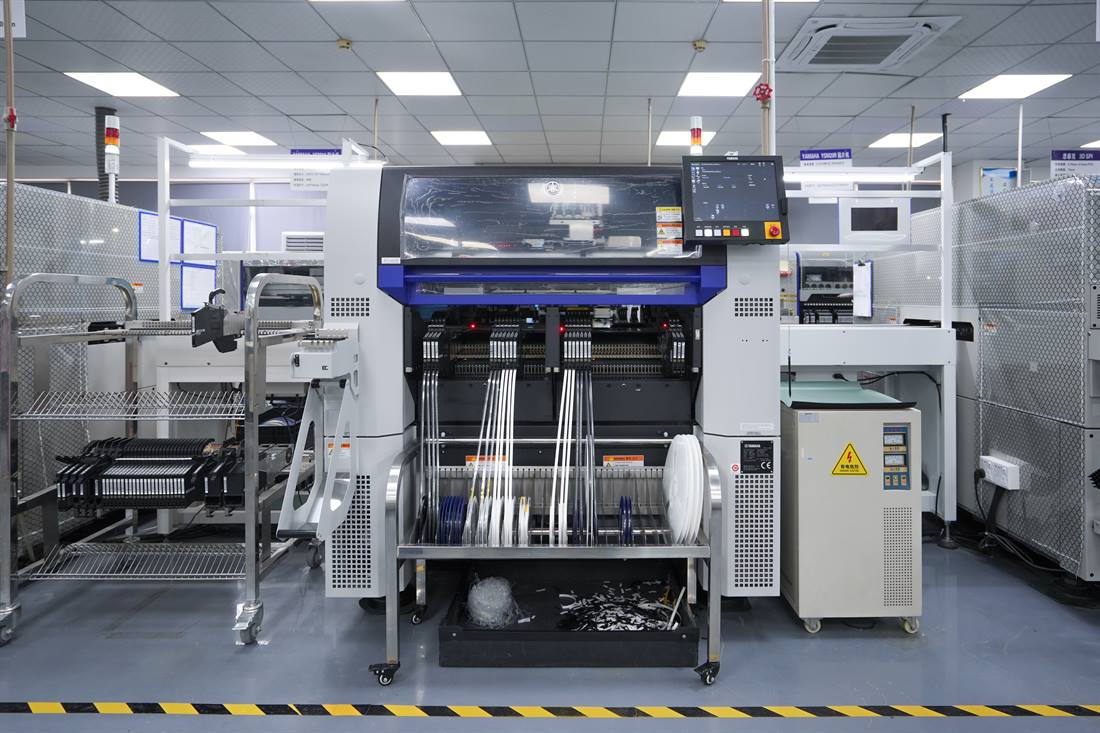
Yamaha placement equipment supports controlled SMT production for prototype, pilot and repeat PCBA builds.
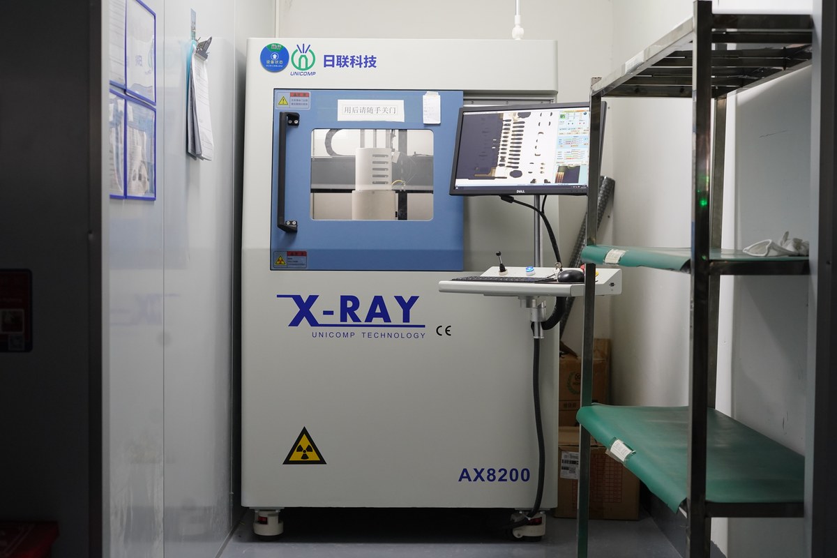
X-ray, AOI, first article and testing evidence help quality teams evaluate process readiness.
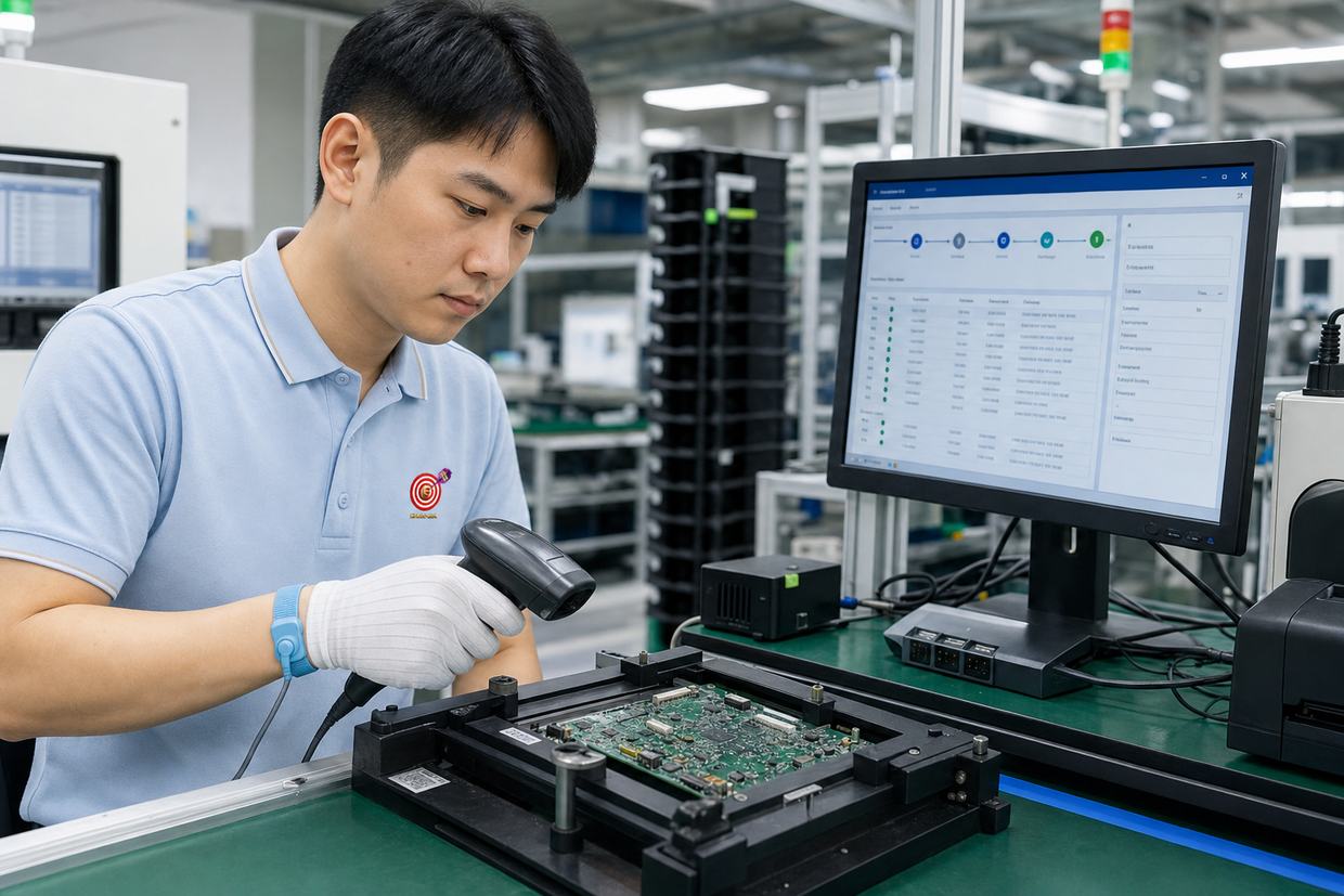
MES and inspection records support the approval process from prototype review to repeat production.

A project engineer coordinates DFM, process and quality input from file preparation through assembly, inspection and testing. Open questions and proposed changes are returned for your approval before production.
Footprint and library mismatches can cause assembly defects or production delays even when automated DRC checks pass. DFM findings identify the affected locations and recommended corrections.
Review incomplete part numbers, availability, lifecycle status and proposed alternatives before components are ordered.
SPI, AOI and X-ray inspection are matched to package and solder-joint risks, with acceptance requirements agreed before shipment.
Confirm materials, approved files, test inputs and production requirements before release. Your quotation identifies the schedule and any open dependencies.
Manufacturing scope, inspection coverage and delivery timing are confirmed for your order.
A DFM report example for a 12-layer control board records manufacturability findings with affected locations and recommended corrections. Review the sample report to see how issues are documented before assembly.

Request a sample DFM report or send your design files for engineering review.
Move from engineering review through prototype, pilot build and volume production. Materials, construction, test development and order quantity determine the schedule confirmed in your quotation.
Confirm files, BOM, construction, assembly requirements and the inspection or test plan.
Build the agreed prototype quantity and record manufacturing, inspection and test findings.
Verify approved changes, repeatability, fixtures and the production documentation needed for the next build.
Manufacture from the approved baseline, with inspection, traceability and shipment requirements defined for the order.
PCB fabrication, sourcing, assembly and testing are coordinated within one manufacturing program.
Meet the specialists supporting PCB manufacturing, component review, assembly processes, inspection, testing and product integration.

Product Design & Development Engineer
PRODUCT DESIGN TEAM
Capability: Product Design & Development
Focus: Product architecture, schematic design, PCB layout, component selection, design verification and prototype support

PCB & PCBA DFM Engineer
DFM ENGINEERING TEAM
Capability: Manufacturability Review
Focus: PCB fabrication and assembly feasibility, footprint verification, solderability review and production-risk identification

PCB Engineering Specialist
ADVANCED PCB TEAM
Capability: Advanced PCB Engineering
Focus: CAM preparation, stack-up, impedance, HDI, material selection and special-process feasibility

Component & BOM Engineer
COMPONENT ENGINEERING TEAM
Capability: BOM & Component Review
Focus: BOM verification, package confirmation, component selection, alternative-part evaluation and lifecycle-risk analysis

SMT Process & NPI Engineer
SMT & NPI TEAM
Capability: New Product Introduction
Focus: Stencil and fixture review, SMT programming, reflow profiling, pilot builds and yield improvement
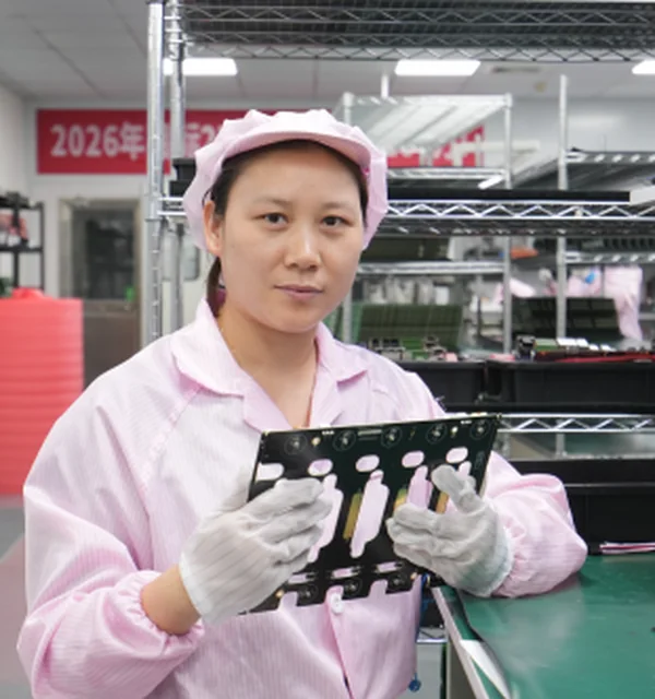
Test & Failure Analysis Engineer
TEST ENGINEERING TEAM
Capability: Testing & Troubleshooting
Focus: Firmware programming, ICT and functional testing, fixture development, defect isolation and root-cause analysis
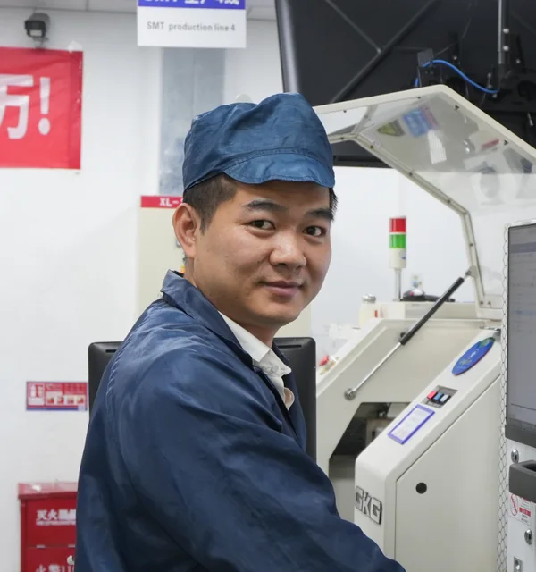
PCBA Quality & Reliability Engineer
QUALITY ENGINEERING TEAM
Capability: Quality & Reliability Assurance
Focus: SPI, AOI, X-ray and first-article inspection, process control, reliability verification and 8D corrective actions

Box Build & Product Integration Engineer
PRODUCT INTEGRATION TEAM
Capability: Complete Product Assembly
Focus: Cable and mechanical assembly, product integration, firmware programming, functional verification and final packaging
MES-linked records can connect agreed board identifiers with material lots, process information, inspection and test results. Record fields, reflow data and retention requirements are confirmed for your order.
Production records can be retained according to the agreed project and quality requirements.
Explore PCB layouts, board constructions, assembly requirements and box-build integration examples. Final manufacturing scope follows the approved project files.
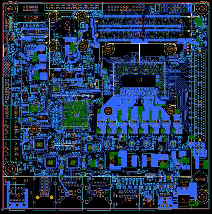
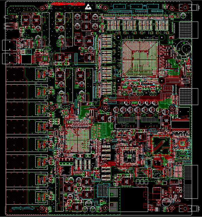
Compact industrial motherboard layout supporting Intel processor options and production interfaces.
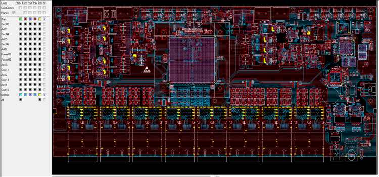
High-density network-board layout built around switching, memory and high-current requirements.
High-speed multilayer layout for dense optical-network connectivity and controlled differential routing.
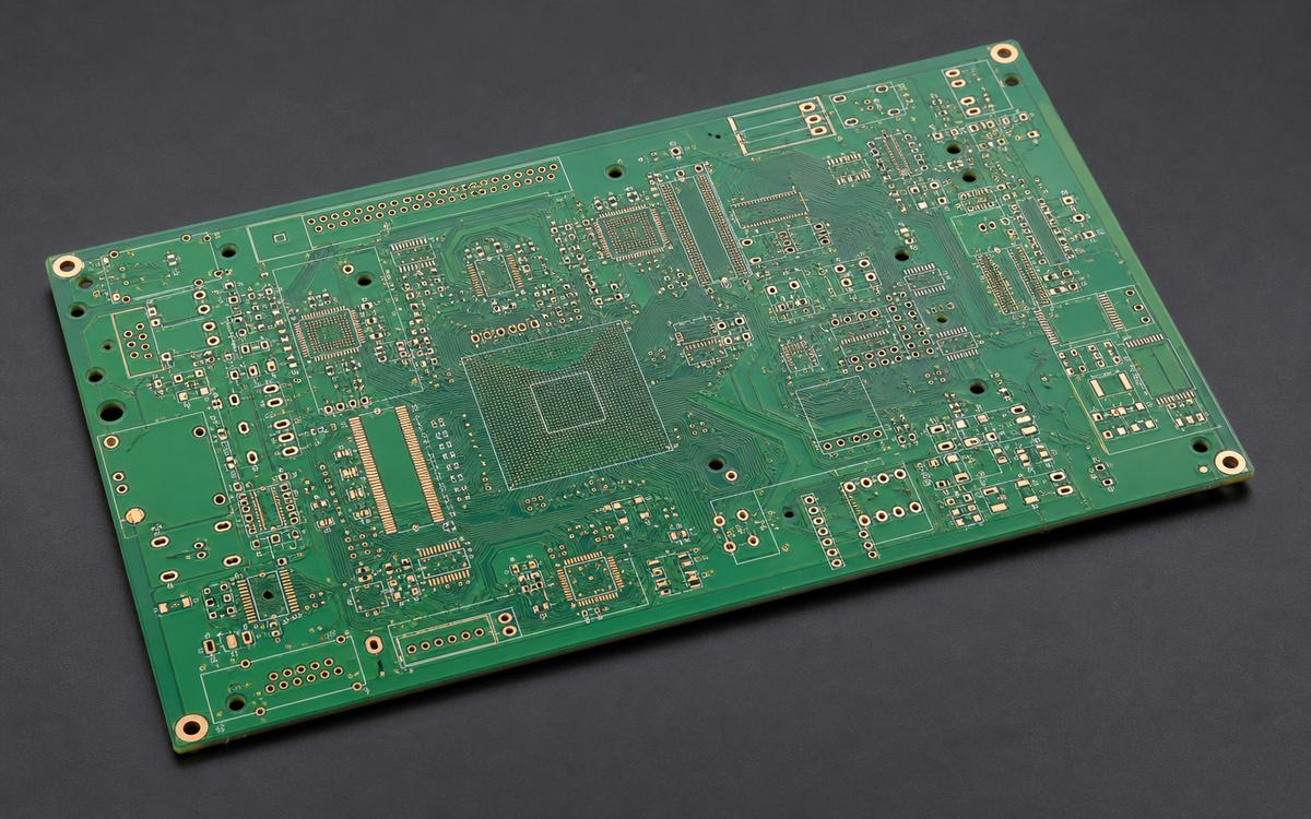
A routine-production route for industrial, telecom and control boards.
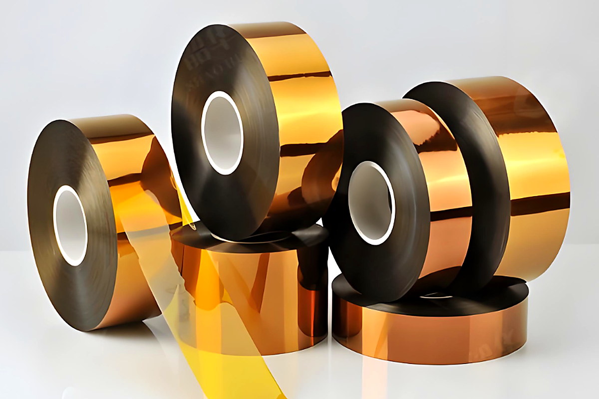
Flexible-board manufacturing for compact interconnect and motion-sensitive assemblies.
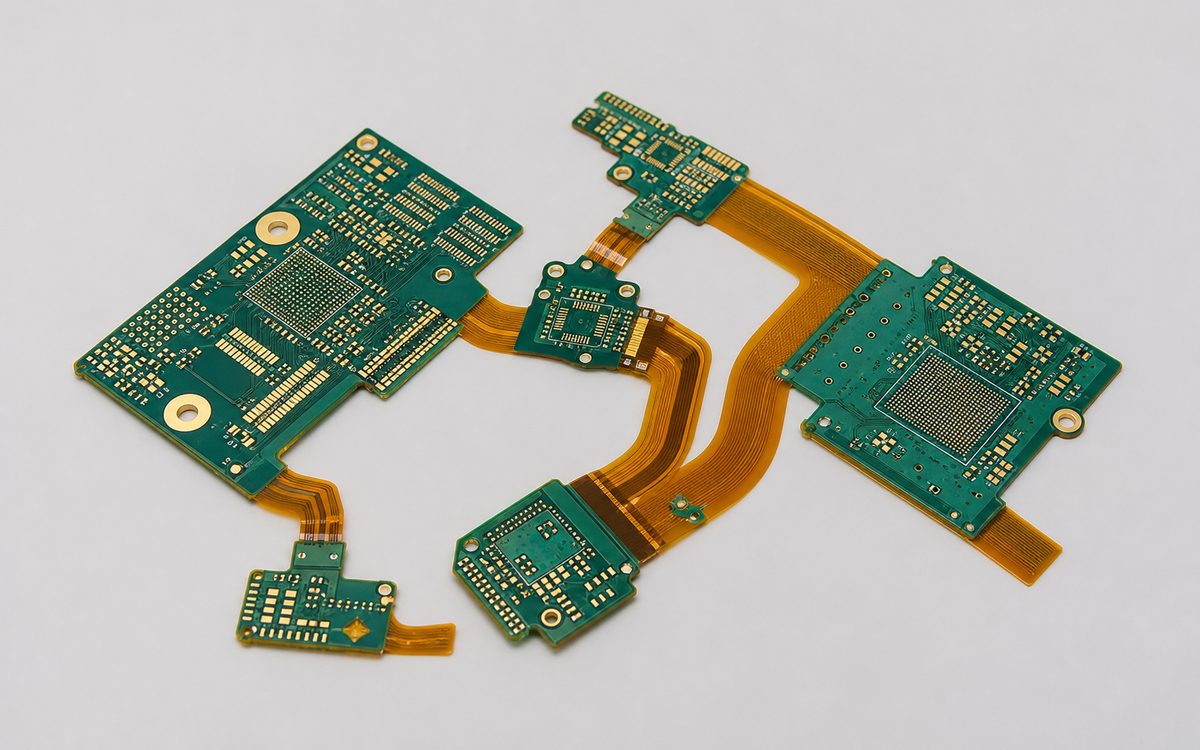
Integrated rigid and flexible construction for space-constrained, connector-sensitive products.
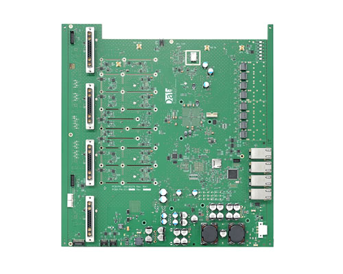
Documentation and repeatability controls prepared before production scale-up.
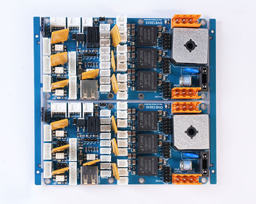
Placement and hidden-joint risks made visible before production release.
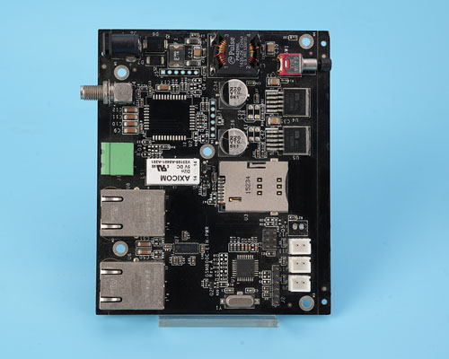
SMT, THT and test requirements coordinated as one controlled build.
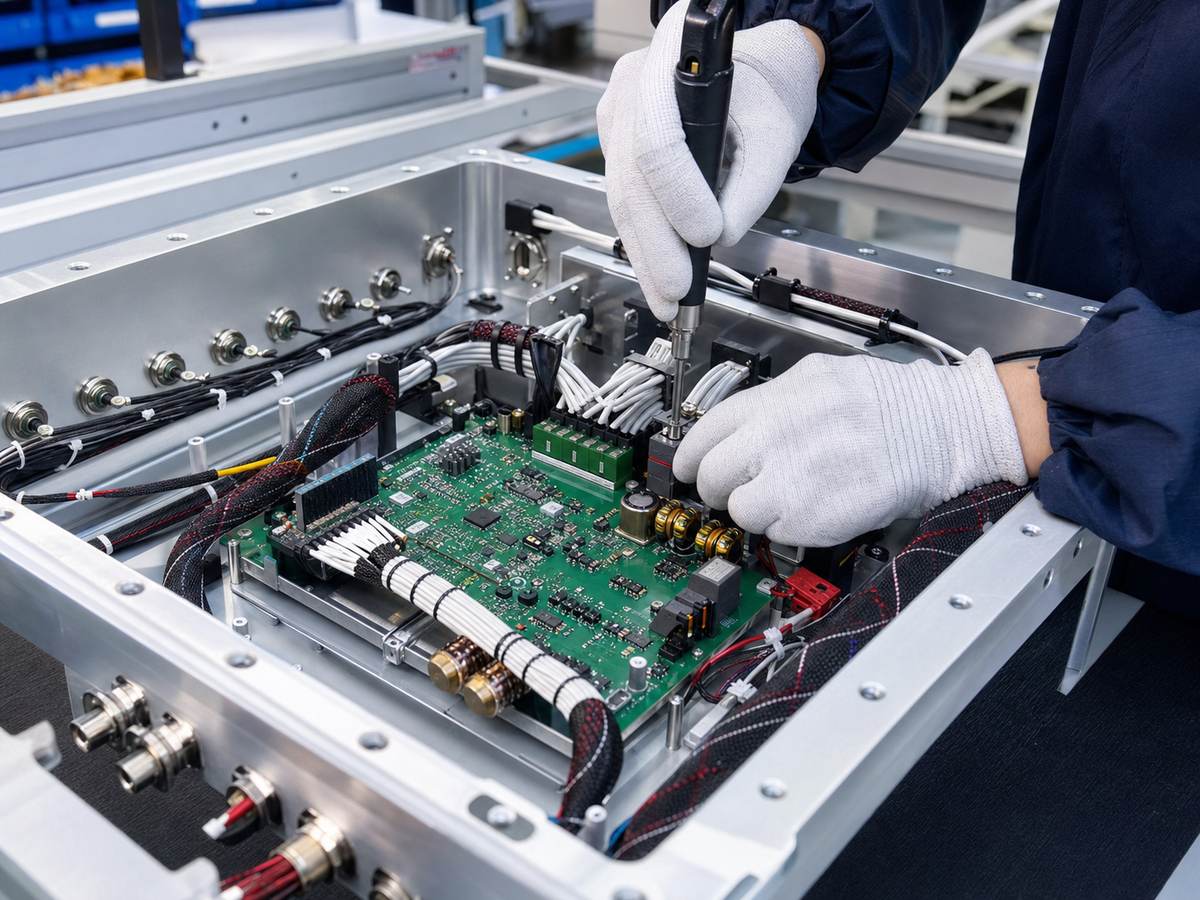
Multi-board enclosure integration with cable routing, firmware loading and finished-unit acceptance.
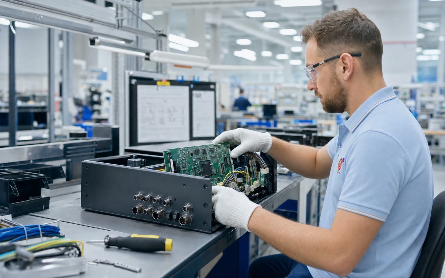
Serialized product integration with coating, controlled revisions and record retention.
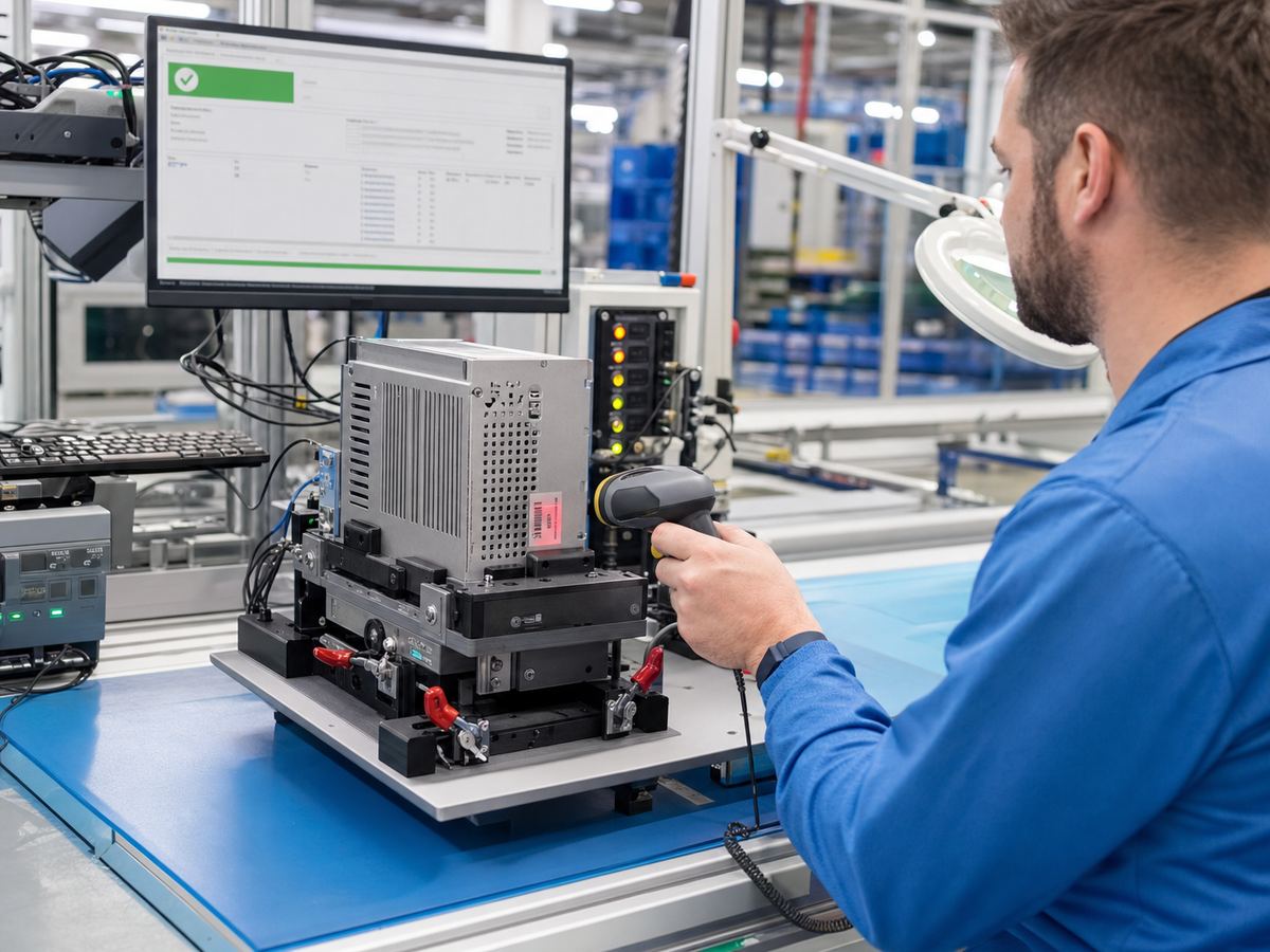
Mechanical and electrical integration where handling, fixture access and packaging define the route.
Share your files and acceptance requirements to receive a project-specific manufacturing, inspection and quotation route.
This medical electronics project required 100 pieces of 16-layer rigid-flex PCBs. The main manufacturing requirements included controlled impedance, tightly controlled thicknesses in the rigid and flex sections, IPC-6012 Class 3 acceptance criteria and four-wire electrical resistance testing.
Review a Similar Project →This order specified an RO4003 / RO4450 construction with 2 oz finished copper and resin-filled vias in component pads. Fabrication data required customer approval before production, with individual boards supplied without tooling rails.
Review a Similar Project →This PCBA project's bare-board requirements combined 6 oz copper with a specified dielectric thickness. The customer prohibited added copper fill in unused circuit-layer areas and required production-data approval before manufacture.
Review a Similar Project →PCB fabrication, component sourcing, assembly and testing are coordinated with dedicated engineering support and clear project requirements.
Certificate copies are available for supplier review. Confirm the certificate holder, site, scope and validity relevant to your order.
PCB and PCBA manufacturing for medical, aerospace, automotive, industrial control, communications, UAV, new energy and robotics applications. Production, inspection and documentation requirements are confirmed for each project.

Patient monitors, diagnostic instruments, imaging modules, medical control units

Flight controllers, ESC & power boards, RF/datalink, IMU sensor modules

Avionics modules, power conversion, high-reliability control electronics under AS9100D
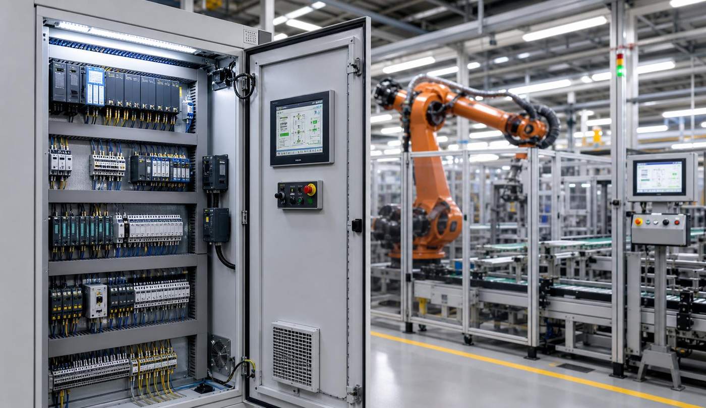
PLC & automation controllers, motor drives, long-format sensor/LED bars to 1,200 mm

Power modules, control units, sensors, vehicle communication systems

RF modules, network interface cards, router & gateway boards

Solar inverter controls, BMS assemblies, energy storage & EV charging
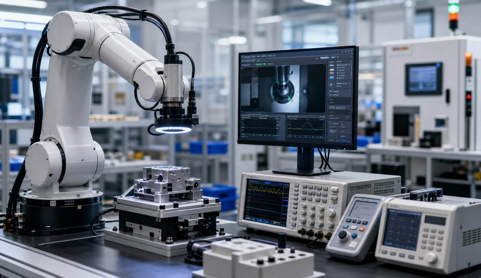
Test & measurement boards, robot controllers, embedded vision modules
Our China facilities cover PCB fabrication, ceramic substrates, SMT, testing and box build. Vietnam supports SMT production, while the US office supports communication with North American customers.
Request an NDA before sharing confidential Gerber files, BOM, drawings or product information. File access and manufacturing responsibilities are agreed for your project.
Request a mutual NDA or submit your company template for review before confidential files are exchanged.
Confirm file access, authorized recipients and the document controls needed for your manufacturing project.
State any confidentiality, tooling ownership or supply-chain restrictions so responsibilities can be agreed before production.
Send your Gerber files, BOM, assembly drawings and target quantities to sales@ebestpcba.com. Our engineering team can review manufacturing requirements and provide quotation guidance for your project.
Request a PCB & PCBA Quote Email Your Project Files