
Suitable for many commercial and industrial products where cost, availability, and standard assembly requirements are the main considerations.
Home / Capabilities / FR4 & Multilayer PCB
FR4 PCB manufacturing
FR4 & Multilayer PCB Manufacturing
EBest PCBA manufactures FR4 PCBs for prototypes and production, with material selection, multilayer stack-up, controlled impedance and surface finishes matched to your design. Send your board files, quantity and delivery target for a fabrication quote.
We aim to provide an initial response within 12 hours. Pricing and production lead time are confirmed after reviewing your files and requirements.
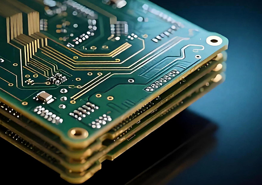
Routine Layers1–10 layersStandard FR4 production range
Higher-Layer BuildsUp to 50 layersSubject to stack-up review
Inner / Outer Copper0.5–3 oz / 1–4 ozReference copper ranges for inner and outer layers
Heavy Copper5–10 ozOn approved constructions
Manufacturing capability
FR4 & Multilayer PCB Manufacturing Capabilities
Compare your design with the ranges below. Copper, holes, line geometry and stack-up are confirmed as a complete construction.
| Capability | Production Reference | Details to Confirm |
|---|---|---|
| FR4 materials | Standard Tg 130–140°C; mid-Tg 150°C; high-Tg 170–180°C. | Material grade, Tg test method, halogen-free requirements and specialty options. |
| Layer count | 1–10 layers for routine builds. | Higher-layer constructions up to 50 layers require stack-up and registration review. |
| Inner-layer copper | 0.5–3 oz reference. | 5–10 oz heavy-copper constructions by review; copper definition and available weights confirmed. |
| Outer-layer copper | 1–4 oz reference. | 5–10 oz by review; base foil, finished copper, etching and plating balance confirmed. |
| Finished thickness | Approximately 0.4–3.5 mm. | Final stack-up, tolerance and thinner or thicker constructions. |
| Finished hole | 0.20 mm minimum reference. | 0.15 mm by review; plating, drill compensation and aspect ratio. |
| Through-hole aspect ratio | Up to 8:1 reference. | Up to 10:1 by review; board thickness and hole diameter must be compatible. |
| Line width / spacing | 4 / 4 mil at 1 oz copper reference. | 3 / 3 mil by review; layer-specific copper and etching requirements. |
| Surface finish | OSP, lead-free HASL, immersion tin, immersion silver, gold fingers, ENEPIG and ENIG. | Mixed finishes by review. |
| Controlled impedance | Manufacturing with an agreed stack-up and impedance requirements. | Trace geometry, dielectric data, coupon design, test method, tolerance and reporting. |
Values are design references, not independently combinable limits. The quotation confirms the material, stack-up, copper, geometry, tolerances and inspection scope for your board.
Materials and stack-up
Material Selection for Your FR4 Build
Choose standard, mid-Tg or high-Tg FR4 according to the assembly profile, operating environment and reliability requirements. Halogen-free and customer-specified grades are reviewed for availability and processing compatibility.
Material grade selected for the assembly profile, thermal requirements and dimensional stability of the build.
Selected when halogen-free compliance is required, subject to laminate availability and electrical requirements.
Customer-specified grades are checked for availability and compatibility with the board construction.
We align layer count, dielectric thickness, copper weight and board thickness with routing, impedance and fabrication requirements. Your approved stack-up defines the production construction.
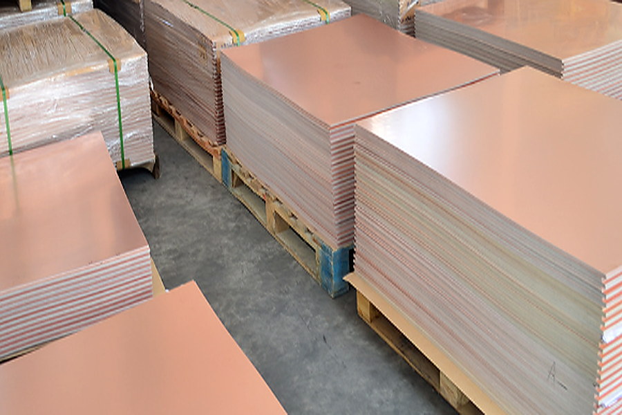
Impedance and stack-up engineering
Controlled Impedance for Multilayer PCBs
Send the target impedance, tolerance, layer assignment and reference planes. We confirm trace geometry, material data and dielectric thickness, then agree the coupon and verification method before fabrication.
Board DataGerber or ODB++, drill data, stack-up, impedance table, fabrication drawing and target quantity
Stack-UpMaterial family, dielectric thickness, copper weight, trace geometry, reference plane and tolerance interaction
VerificationTarget impedance, tolerance, coupon design, measurement method and agreed reports
Production DataApproved production files, file revision, and required inspection records
Manufacturing control
FR4 PCB Manufacturing Process
From approved fabrication data to finished boards, the process follows the agreed material, stack-up and inspection requirements.
Fabrication Data and Stack-Up
Review fabrication data and approve the stack-up.
Inner-Layer Circuits
Image and etch inner layers.
Lamination, Drilling and Plating
Laminate, drill and plate the approved construction.
Outer-Layer Circuits and Solder Mask
Form outer-layer circuits and apply solder mask.
Surface Finish and Profiling
Apply the specified finish and profile the boards.
Electrical Testing and Final Inspection
Complete electrical testing and agreed final inspection.
PCB manufacturing options
FR4 PCB Builds We Support
Explore FR4 board constructions for control electronics, signal integrity and thermal requirements.
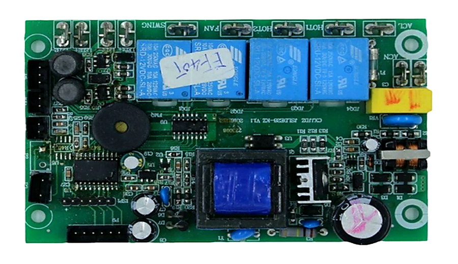
Industrial control profile
Multilayer Control Board
Routing, power distribution and production documentation matched to the approved stack-up.
- Manufacturing Requirements
- Stack-up, copper balance, drill and panel utilization
- Inspection Records
- Electrical test and agreed final inspection records
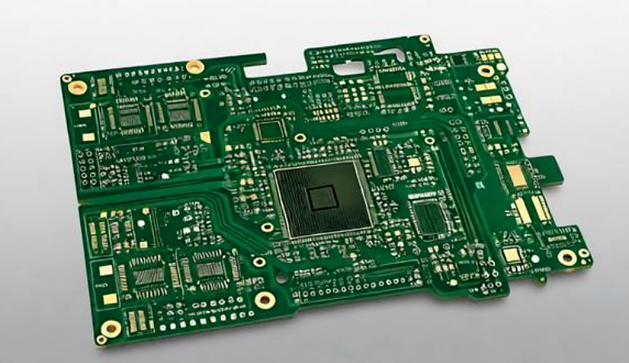
Signal-integrity profile
Controlled-Impedance Multilayer
Layer-specific geometry, reference planes and verification requirements defined before fabrication.
- Manufacturing Requirements
- Impedance table, finished geometry and coupon strategy
- Inspection Records
- Agreed impedance and electrical-test records
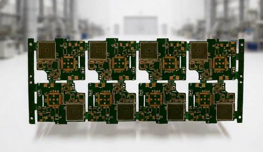
Thermal-duty profile
High-Tg FR4 Construction
Material grade selected for the assembly profile and service environment.
- Manufacturing Requirements
- Tg family, thermal profile, thickness and material approval
- Inspection Records
- Material and inspection records agreed at quotation
Assembly handoff
Surface Finish Options
Surface finish affects solderability, flatness, shelf life, fine-pitch assembly, contact performance, compliance, and cost. Select the finish together with the PCB design, assembly process, storage requirements, and product environment.
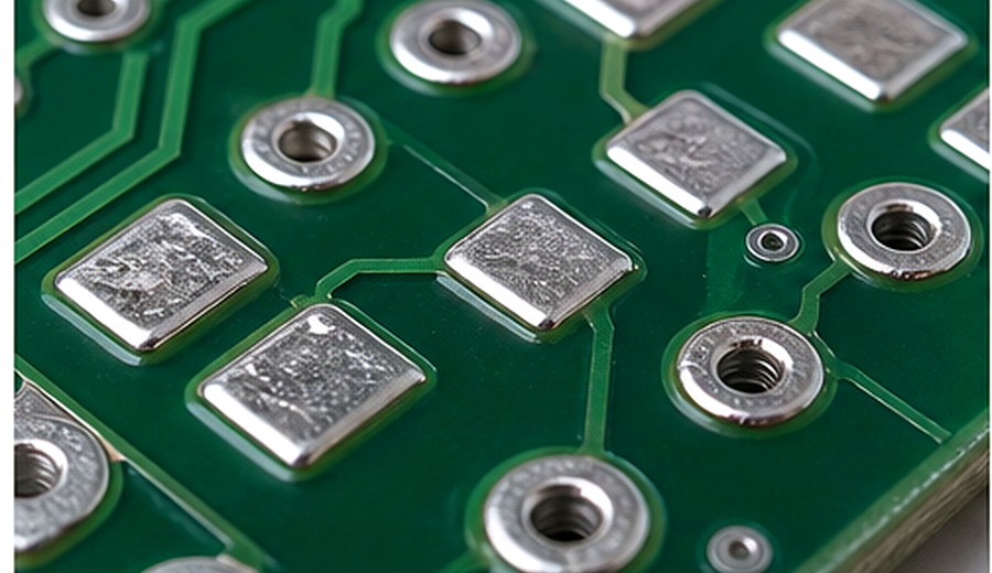
Lead-Free HASL
For assemblies that tolerate pad-height variation.
CHECK: flatness, fine-pitch suitability and thermal exposure
ENIG
A flat finish for fine-pitch soldering, with plating requirements defined.
CHECK: gold thickness, nickel system and product environment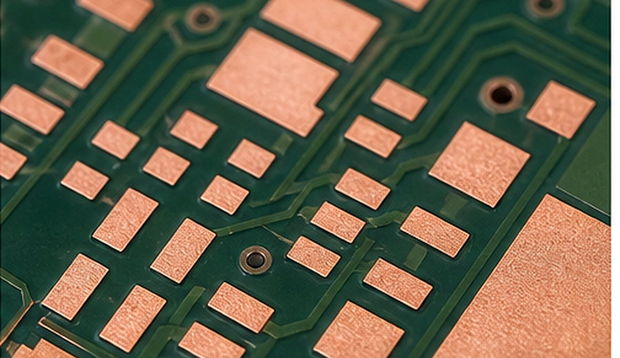
OSP
Flat copper protection with controlled handling and assembly timing.
CHECK: shelf life, handling and assembly sequence
Immersion Silver
Confirm packaging, storage and environment.
CHECK: packaging, storage and operating environment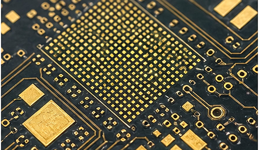
ENEPIG
Review the specific soldering or wire-bonding process.
CHECK: application, specification and availability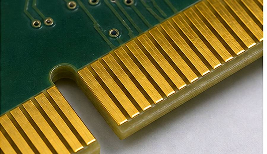
Gold Fingers
Specify contact area, hard-gold requirements, thickness and bevel on the drawing.
CHECK: contact drawing, bevel and wear requirementQuote-ready review
What to Send for an FR4 PCB Quote
Send the files you have. We will identify missing details and confirm the fabrication scope, price and lead time.
Board dataGerber or ODB++, NC drill and netlist when available
Fabrication drawingDimensions, tolerances, finish, marking and mechanical notes
Stack-up and impedanceProposed stack-up, impedance targets, tolerances and reference layers
Material requirementMaterial grade, Tg family, copper weights and compliance requirements
Quantity & Lead TimePrototype, pilot or production quantity and target schedule
Inspection & Test RecordsElectrical, impedance, microsection or other agreed records
FAQ
FR4 & Multilayer PCB FAQ
What layer counts can EBest PCBA review?
Routine FR4 builds cover 1–10 layers. Higher-layer constructions up to 50 layers require review of the stack-up, material, registration and inspection requirements.
What files are needed for a PCB quote?
Send Gerber or ODB++, drill data, the fabrication drawing, quantity and any stack-up, material, impedance or finish requirements. A review can begin with partial data.
Can you manufacture controlled-impedance PCBs?
Yes, subject to stack-up review. We agree the impedance target, tolerance, trace geometry, reference planes, coupon and verification method before production.
Which FR4 material options can be reviewed?
Standard, mid-Tg, high-Tg, halogen-free and customer-specified grades can be reviewed. Material selection depends on assembly conditions, service requirements and availability.
What inspection records are available?
The agreed quality plan defines the records provided. Electrical test results, dimensional records, impedance reports and microsections can be discussed before ordering.
Can fabrication be combined with turnkey PCBA?
Yes. Send the BOM, placement data and test requirements so PCB fabrication, sourcing, assembly and testing can be planned together.