
Rigid islands in one build
Connect component areas without using separate PCBs and cables for each section.
Combine rigid component areas and flexible interconnects in one PCB for compact assemblies. EBest PCBA reviews the rigid and flex stack, transition zones, via structure and assembly requirements to prepare your fabrication quote.
We aim to provide an initial response within 12 hours. Final construction, inspection scope, pricing and production lead time are confirmed after file review.
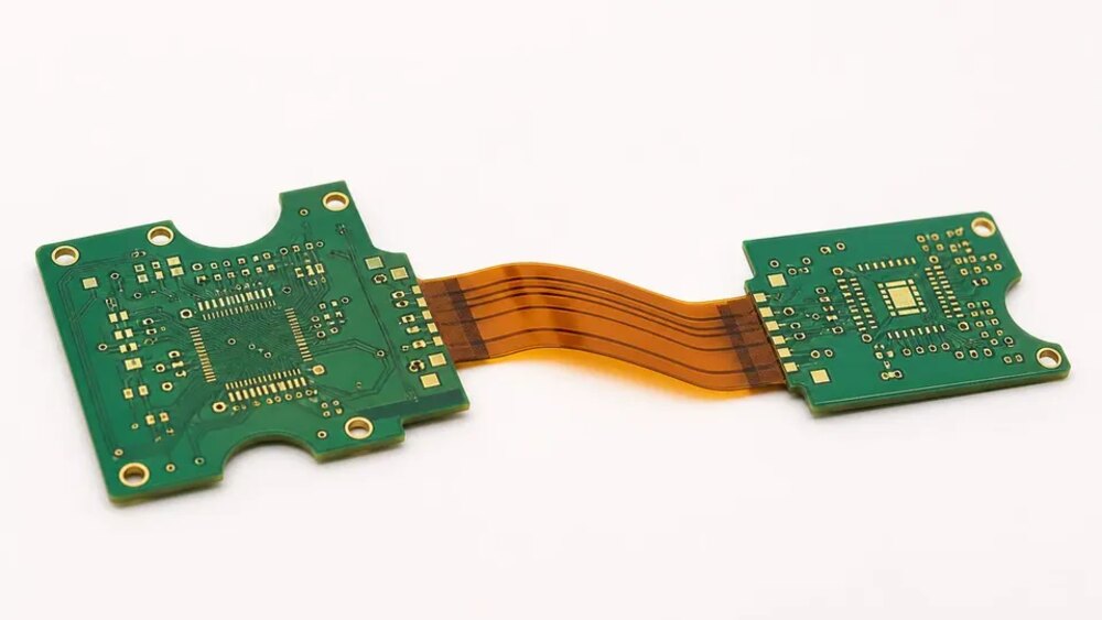
Rigid-flex can reduce separate board-to-board connections and support compact three-dimensional layouts. The design still needs approved bend conditions, transition geometry, mounting support and assembly access.
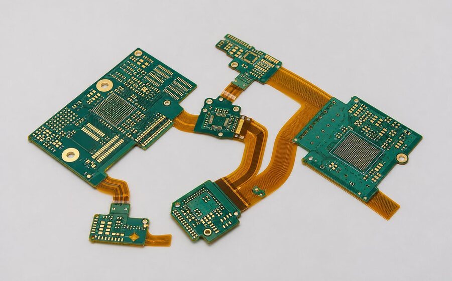
Connect component areas without using separate PCBs and cables for each section.
Confirm bend radius, fold direction, trace direction, and mechanical keep-outs before fabrication.
Replace selected cables and connectors with integrated flex interconnects where the product design allows.
Review carriers, connectors, component keep-outs, and flex handling before PCBA assembly.
The complete rigid-flex stack and mechanical requirements determine the approved construction. Compare the references below with your regional thickness, routing and assembly needs.
| Capability | Production Reference | Conditions / Special Review |
|---|---|---|
| Layer count | 2–10 layers for routine constructions | Higher-layer constructions up to 50 layers, subject to review of the complete stack-up, registration, materials and via structure. |
| Flex-layer position | Outer-layer and middle-layer options | Position follows the approved copper, coverlay, bend conditions and assembly sequence. |
| Manufacturing thickness | 0.30–4.0 mm reference | The finished-board range does not define flex-region thickness. Rigid, flex and reinforced regions are specified separately in the approved stack-up. |
| Regional thickness | Rigid and flex thicknesses defined separately | One supported route lists rigid areas at 0.25–3.0 mm and flex areas from 0.13 mm. Final regional thicknesses and tolerances are confirmed for the selected construction. |
| Minimum flex-region width | 2.0 mm reference | This is a region-width reference, not a bend-radius limit. Mechanically constrained regions require review. |
| Finished size | Minimum: 5 × 10 mm; maximum: 500 × 500 mm on supported constructions | Separate long-board routes list 210 × 780, 210 × 800 or 210 × 1000 mm; selected builds up to 210 × 1100 mm require review. Size limits belong to their respective production routes. |
| Conductor thickness | 0.5–2 oz reference (18–70 μm) | Applies to selected constructions; base copper, finished copper, minimum geometry and bend requirements are confirmed together. |
| Adhesive polyimide core | PI: 0.5, 1 and 2 mil; copper: 0.33, 0.5 and 1 oz | Other material grades and combinations subject to availability and stack-up review. |
| Adhesiveless polyimide core | PI: 0.5, 1, 2 and 3 mil; copper: 0.33, 0.5, 1 and 2 oz | Material family, copper type and bend suitability confirmed with the construction. |
| Flex dielectric thickness — excluding copper | 12, 18, 25, 50, 75, 100, 125 and 150 μm | FCCL dielectric options; adhesive and coverlay thicknesses are defined separately. |
| Rigid laminate | FR4 grades selected for the design | Special rigid materials reviewed for availability and thermal, electrical and processing compatibility. |
| Rigid core thickness — excluding copper | 0.10, 0.12, 0.15, 0.20, 0.25, 0.30, 0.40, 0.50, 0.60, 0.80, 1.0, 1.2, 1.6 and 2.0 mm | CCL core options; these values are not the complete finished-board thickness. |
| Inner-layer line / space — 18 μm finished copper | 3 / 3 mil before compensation | Special process: 2.5 / 2.5 mil; localized 2 / 2 mil features subject to review. |
| Inner-layer line / space — 35 μm finished copper | 4 / 4 mil before compensation | Special process: 3.5 / 3.5 mil; geometry confirmed with copper and stack-up. |
| Inner-layer line / space — 70 μm finished copper | 6 / 8 mil before compensation | Special process: 5.5 / 7 mil; geometry confirmed with copper and stack-up. |
| PTH / NPTH diameter tolerance | PTH: ±3 mil; NPTH: ±2 mil | Finished hole size and acceptance requirements are confirmed on the fabrication drawing. |
| Hole position tolerance | ±4 mil reference | Positioning datums and applicable features are confirmed by drawing. |
| PTH wall copper thickness | 15 μm reference | Hole-wall copper and inspection requirements are agreed for the construction and acceptance standard. |
| Through-hole aspect ratio | 8:1 maximum reference | Applies to supported through-hole constructions; hole type, diameter and regional board thickness are reviewed together. |
| HDI structures | 1+N+1 reference, subject to stack-up review | Higher-order build-ups and special via combinations evaluated against the regional stack and via map. |
| Controlled impedance | Target >50 Ω: ±10%; target ≤50 Ω: ±5 Ω | Impedance targets, applicable regions, coupons and measurement methods are agreed for the approved construction. |
| Coverlay | Shengyi SF305C, Taiflex FHK and DuPont FR series | Film, adhesive thickness and openings selected for the approved stack; availability confirmed before production. |
| Bonding adhesive | 25 μm reference | 10 μm and 40 μm options subject to material and construction review. |
| Low-flow prepreg | 40, 60, 80 and 100 μm options | Grade, thickness and resin movement reviewed around rigid-flex boundaries. |
| PI stiffener | 3, 5, 7 and 9 mil options | Local support, connector fit and total regional thickness confirmed by drawing. |
| Electrical test pad spacing | 4–5 mil minimum | Special process: 4 mil; test access and method confirmed for the design. |
| Surface finish | ENIG, flash gold, gold plating, hard gold fingers, OSP and electroplated tin | Selective gold plating, ENEPIG and ENIPIG subject to project review. Contact areas, coating specifications and regional compatibility are confirmed by drawing. |
Rigid-flex construction should be selected based on how the product will be installed, folded, assembled, and tested. More complex structures may need additional engineering review.
For a defined fold between two supported component areas.
For assemblies with several supported component areas and planned flex connections.
Flex-layer position is selected based on protection, assembly access, copper geometry, and lamination requirements.
For dense routing where the via map and sequential build-up are approved.

The rigid laminate, polyimide, copper, coverlay and bonding materials are selected together. The drawing defines rigid boundaries, flexible areas, local thickness and the assembly envelope.
FR4 and selected special rigid materials are reviewed against thermal, electrical and thickness requirements.
Adhesive or adhesiveless polyimide cores and copper options are selected for the flexible regions.
Low-flow prepreg or adhesive must limit resin movement around rigid-flex transitions and openings.
Coverlay, PI support, local reinforcement and pressure-sensitive adhesive are coordinated with assembly.
Define fold direction, bend radius, clamp positions and static or dynamic use. We check conductor routing, coverlay overlap, resin movement, holes and support around the transition against the approved construction.
We mark affected regions and identify the geometry, material or handling issue that needs clarification. The review covers regional stack-up, transition features, via placement, impedance, bend conditions and assembly support.
Confirms rigid, flexible and adhesive layers, copper weights, coverlay and overall thickness.
Reviews conductor clearance, resin flow, support, openings and corner radii at the boundary.
Check PTH, buried vias, and laser vias against the transition zone, copper construction, and HDI requirements.
Examines trace direction, width changes, bend area, fold orientation and mechanical constraints.
Coordinates trace geometry and dielectric behavior across rigid and flexible stack sections.
Plans tooling, carriers, component keep-outs, connector support and flex handling during PCBA.
Production follows the approved regional stack and fabrication data. Electrical testing and final inspection follow the agreed scope; dynamic bend qualification is specified separately.
Approve the regional stack, fabrication data and bend requirements.
Prepare the selected rigid laminate, polyimide, copper and bonding materials.
Form circuits and interconnections against the approved fabrication data.
Laminate the approved construction and control registration and hole locations.
Apply finish and profile the rigid and flex areas.
Complete electrical testing and agreed dimensional and visual inspection.
Select a construction that fits your component areas, planned folds and assembly requirements.
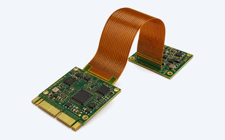
Supported component areas connected through a defined flexible link.
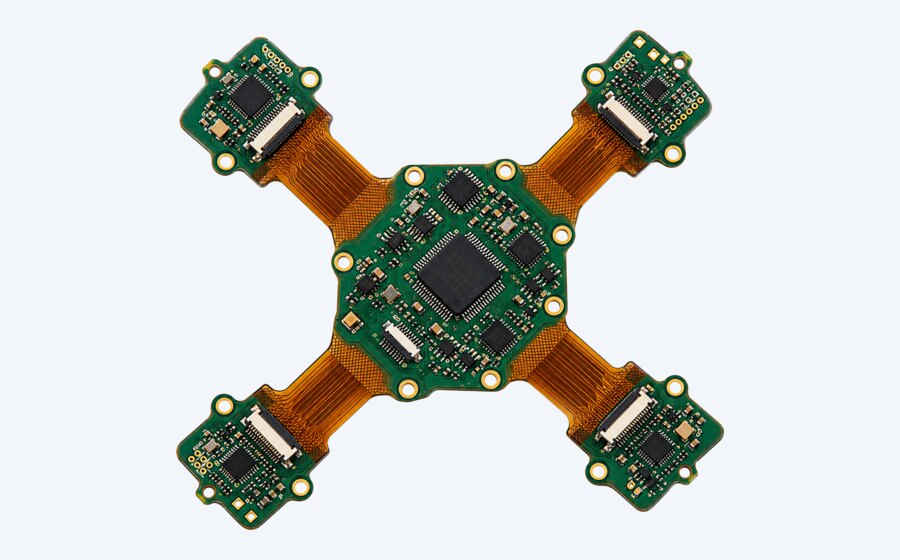
Multiple rigid areas with planned folds, support and assembly clearances.
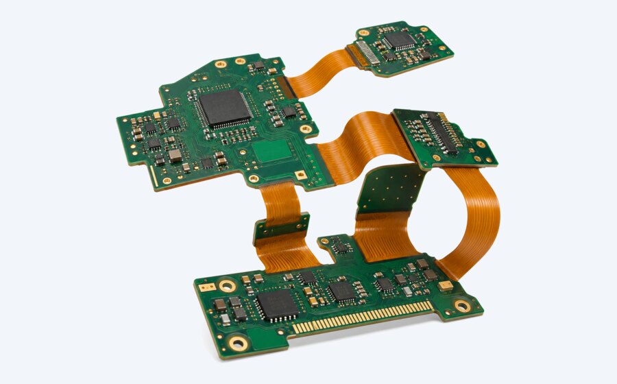
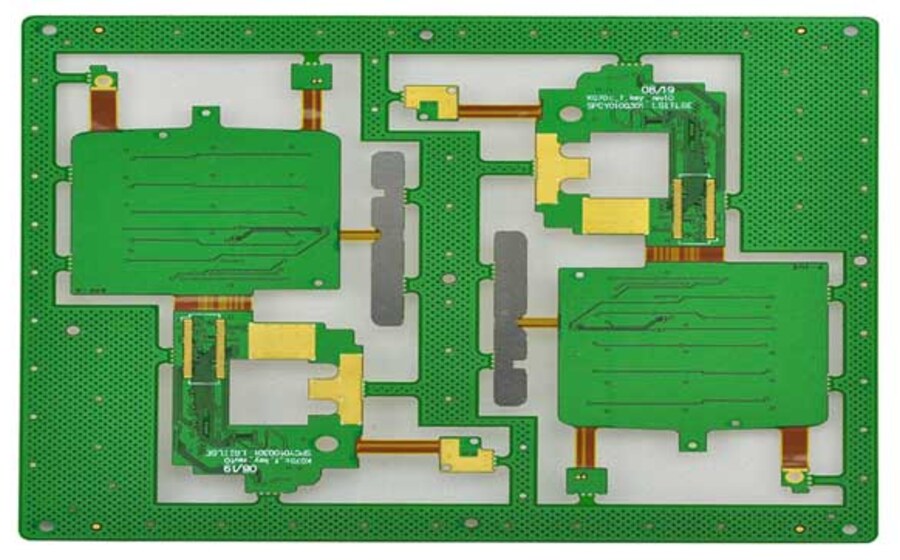
Production panels designed for handling, registration and depaneling of selected constructions.
Share your files and mechanical requirements. We will review the regional stack, transitions and manufacturing plan before confirming pricing and lead time.