
01 / SIGNAL INTEGRITY
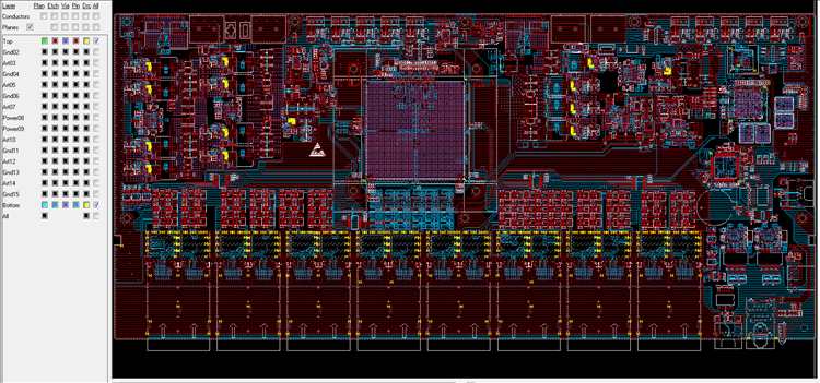
RF & High-Speed PCB Layout
Review stack-up, reference planes, return paths, differential pairs, via transitions, controlled impedance and manufacturing access before release.
Review telecom PCB layout →EBest PCBA provides PCB and PCBA manufacturing for telecommunications electronics, covering controlled-impedance boards, component sourcing, assembly, inspection, and testing for network, optical, RF, and power applications.
 Telecommunications Electronics Application
Keep RF and high-speed layout, controlled-impedance PCB prototyping, low-loss materials, assembly and verification decisions connected for network, optical and telecom power equipment.
Review stack-up, reference planes, return paths, differential pairs, via transitions, controlled impedance and manufacturing access before release.
Review telecom PCB layout →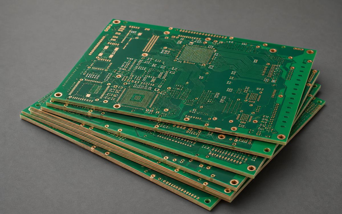
Confirm low-loss material options, stack-up, drill and backdrill strategy, impedance coupons and inspection requirements before repeat builds.
Review telecom PCB prototypes →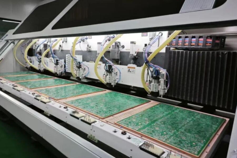
Release approved stack-up, material, copper geometry, impedance, drill, finish, panel and verification requirements as one production baseline.
Review telecom PCB production →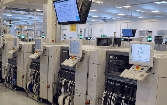
Connect approved components, SMT controls, inspection coverage, programming and project-defined network, optical or power testing to the released PCB.
Review telecom PCBA assembly →Before fabrication starts, review the stack-up, impedance targets, material requirements, via structure, and inspection criteria against the released PCB data. This helps identify manufacturing conflicts before they reach production.

Confirm impedance targets, material data, and controlled-trace requirements against the fabrication files.
Review stack-up and reference-plane requirements that affect controlled-impedance fabrication.
Confirm via structure, stub limits, backdrill depth, and related fabrication tolerances.
Verify specified laminate availability and review any proposed material change before production.
Confirm the required impedance, inspection, test, and production records before release.
The product environment determines the PCB construction, component controls, assembly route and verification evidence—not the industry label by itself.

High-speed digital, RF interfaces, telecom power and outdoor reliability requirements must be reviewed together.

Dense multilayer routing, controlled impedance, connector interfaces and thermal loading drive the construction route.

High-speed interfaces, transceiver placement, low-loss routing and assembly cleanliness require coordinated review.

Throughput, power density, cooling, serviceability and repeat-build continuity shape PCB and PCBA decisions.
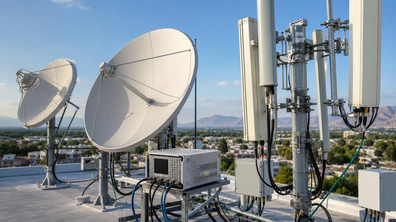
Material properties, transitions, finish, dimensional control and verification method are confirmed for the frequency range.
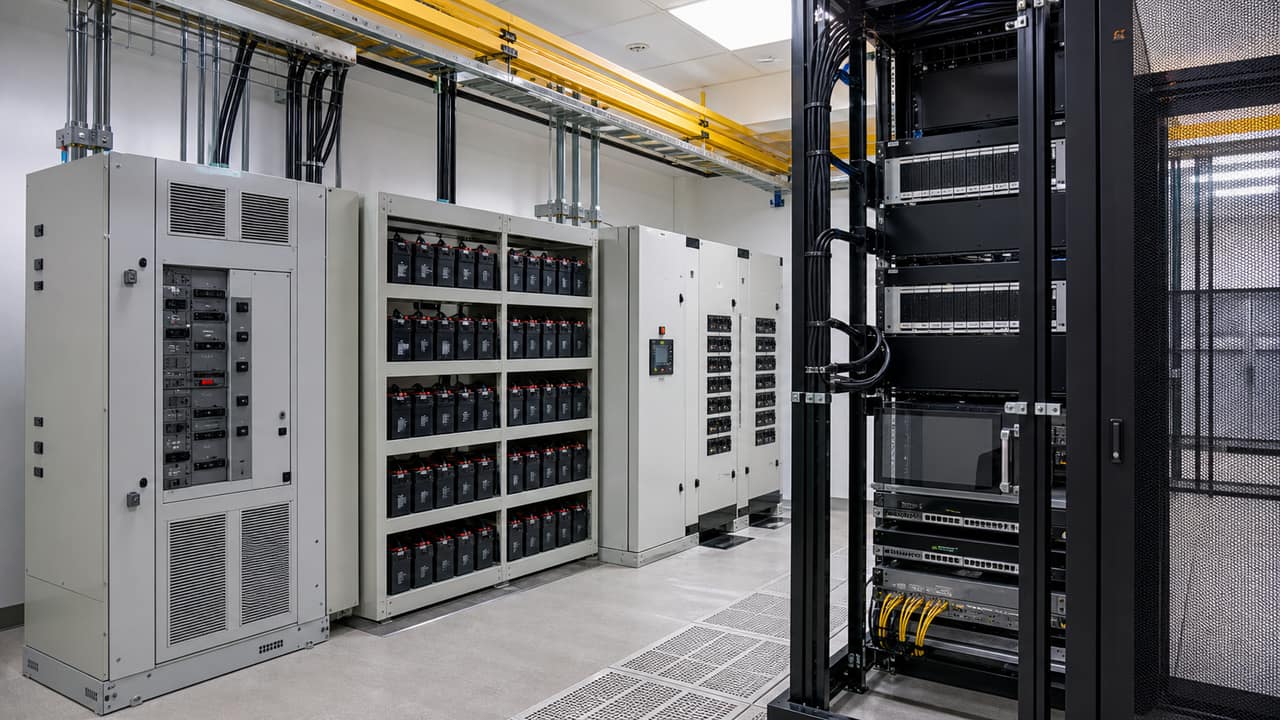
Copper weight, thermal transfer, isolation, component sourcing and functional acceptance require a project-specific route.
Send your approved files and requirements. EBest PCBA confirms the materials, PCB construction and verification scope before quotation.
| Review Area | You Provide | EBest PCBA Confirms |
|---|---|---|
| Project Files | Gerber, BOM and drawings | File completeness and scope |
| Materials & Stack-up | Material and stack-up requirements | Availability and manufacturability |
| Layers & Features | Layer count and layout requirements | Production capability |
| HDI & Backdrill | Via and backdrill requirements | Structure and tolerances |
| Copper & Finish | Copper and finish requirements | Process availability |
| Impedance & Inspection | Impedance and inspection requirements | Test method and records |
Each stage confirms the design requirements, stack-up, materials, sourcing, assembly, inspection, and test scope before the project moves into production.
Check available Gerber/ODB++ files, BOM, drawings, quantities, test requirements, and missing information.
Review materials, impedance, layer structure, trace geometry, routing constraints, and manufacturability risks.
Define approved materials, stack-up, impedance control, copper requirements, tolerances, and inspection criteria.
Review component sourcing, approved alternatives, package requirements, assembly process, and revision control.
Apply the required SPI, AOI, X-Ray, electrical, or functional testing according to the project requirements.
Link the approved revision, materials, inspection results, test records, and traceability information to the production lot.
Explore PCB build routes for high-speed telecom hardware. Final stack-up, materials and inspection requirements are confirmed from your released data.
TEL01 / PROJECT REQUIREMENTS
This HDI order combined blind and buried vias with two impedance targets on four routing layers. The customer requested a manufacturability check of the supplied stack-up and a revised production stack-up if needed.
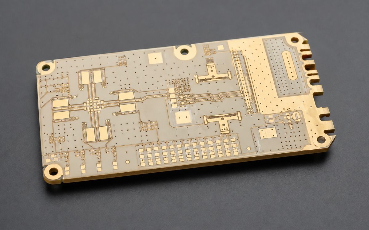
TEL02 / PROJECT REQUIREMENTS
This four-layer order specified hard-gold fingers without beveling and removal of the gold-plating leads. The routing differed from revision A0, so the customer required an EQ review and approval of production data before manufacture.
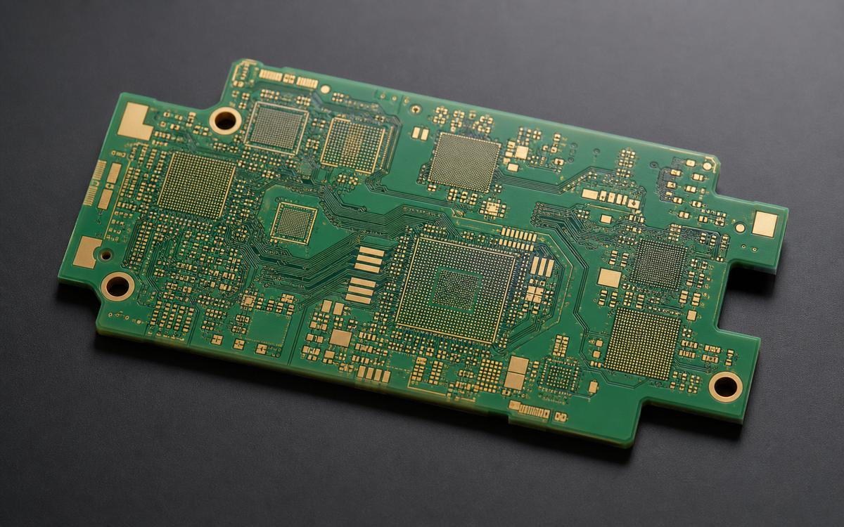
TEL03 / PROJECT REQUIREMENTS
This customer-designated automotive PCB order required equal prepreg thicknesses and copper-paste plugging at the holes identified in the drawing. Production files and stack-up needed approval before manufacture.
TEL04 / PROJECT REQUIREMENTS
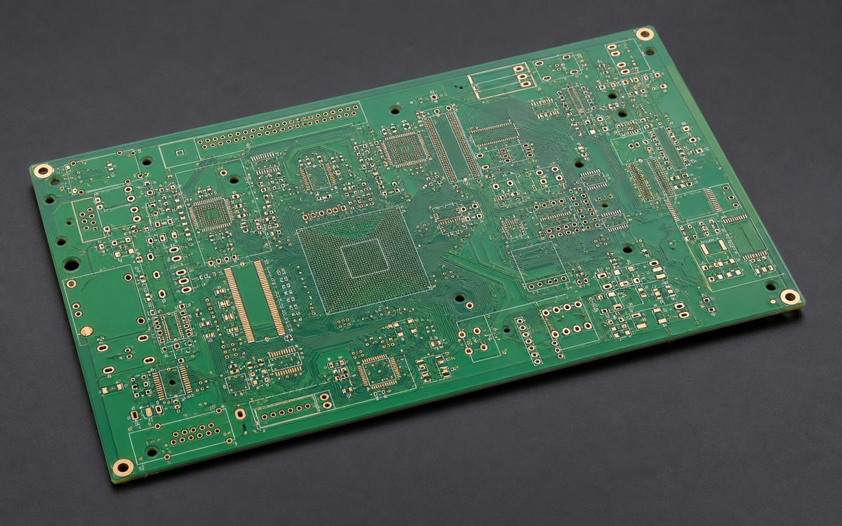
The revised board removed blind vias, increased the dimensions and changed the solder-mask color to black. The order required customer-approved production data, individual-board delivery and shipment inspection reports.
TEL05 / PROJECT REQUIREMENTS
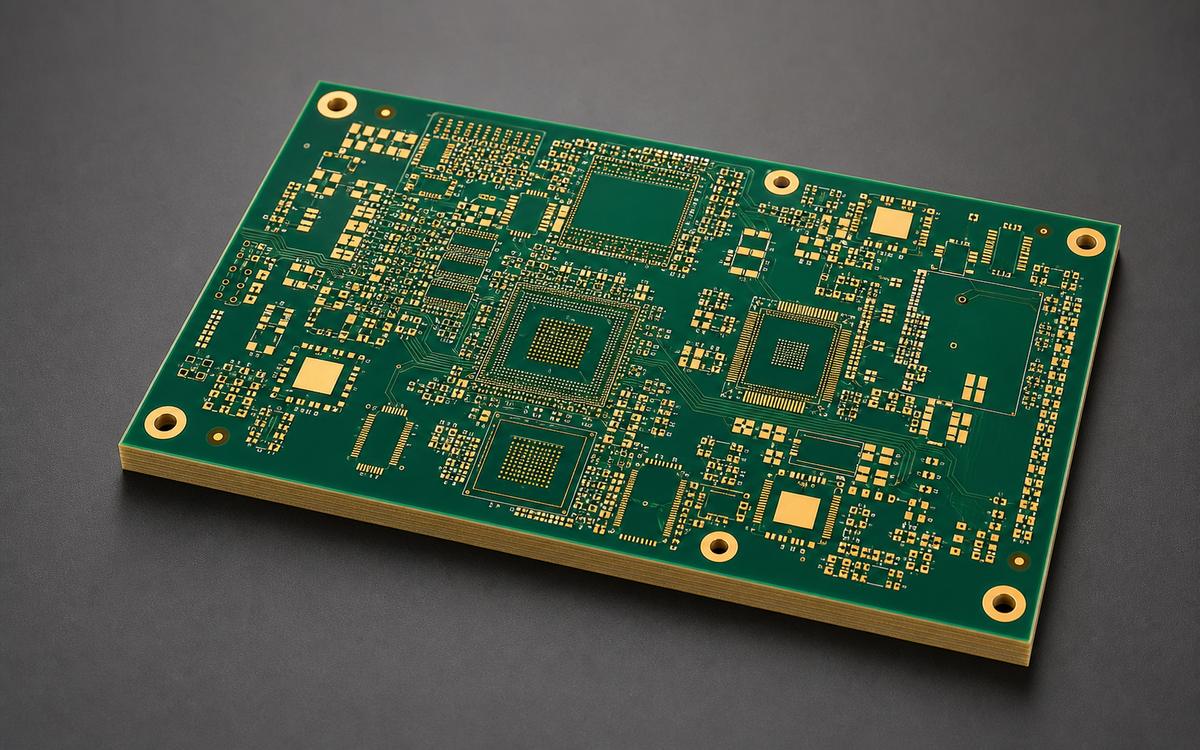
This rigid-flex order specified separate stiffener thicknesses for the flex fingers and rigid region. Adhesive tape and reinforcing adhesive were required at defined interfaces, with customer approval of panel artwork and stack-up before production.
TEL06 / PROJECT REQUIREMENTS
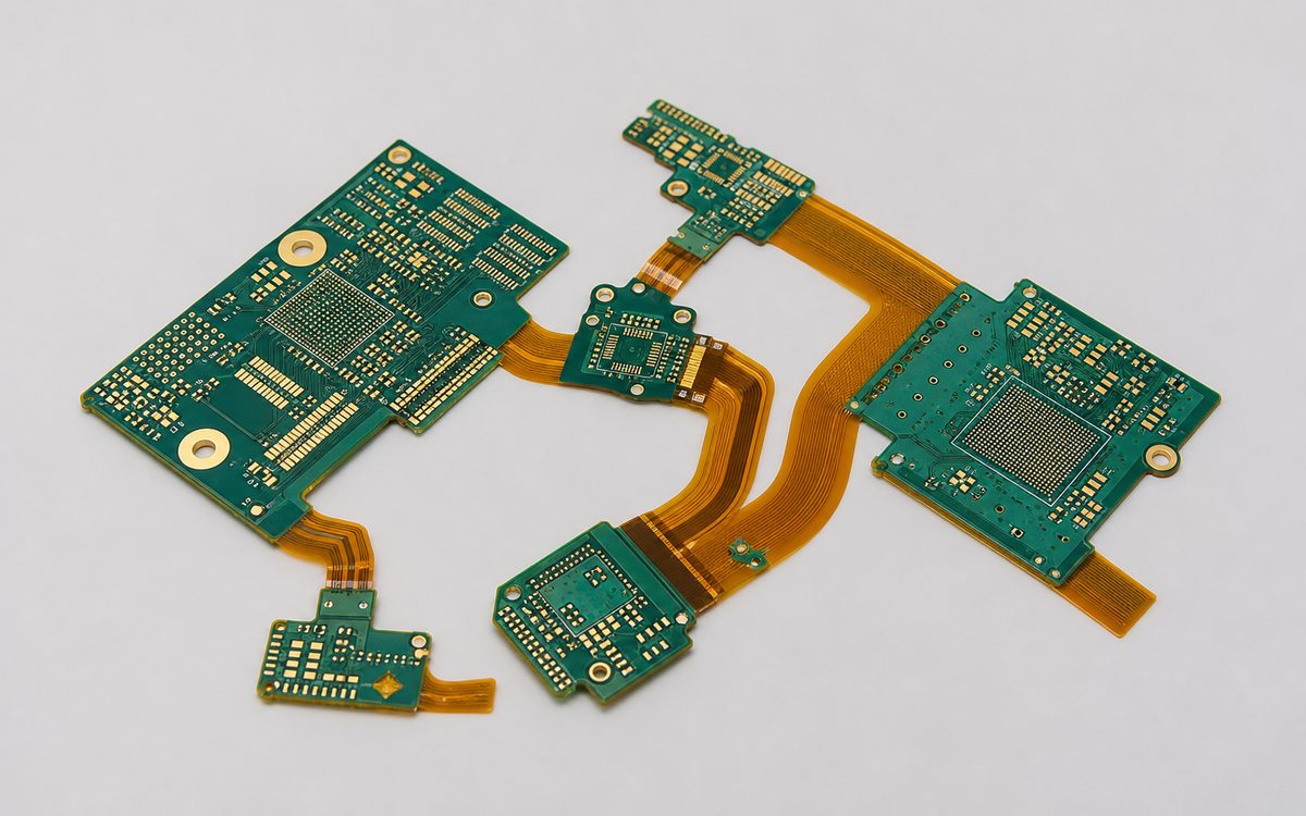
This panelized PCB order required customer-defined QR identification and board-edge fiducials. The printed identifier combines the part number, supplier code, production date, batch and serial number; exact encoding follows the customer attachment.
Before supplier approval, your engineering and quality teams can review the DFM process, PCB and PCBA manufacturing capabilities, inspection and test resources, and relevant quality certifications for your project.

You do not need every answer before contacting EBest PCBA. Send the available files and flag the open questions; engineering will identify the missing inputs before quotation.
Review practical guidance on controlled impedance, materials, stack-up, fabrication limits, inspection, and other manufacturing considerations for high-speed and RF PCB projects.
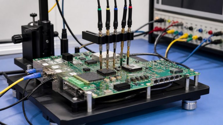
See how we inspect and test telecom PCBAs across solder process, hidden joints, programming, power, data interfaces and customer-defined traffic conditions.
Read article →See how we review RF PCB materials, stack-up, geometry, vias, launches, finish and production evidence before fabrication release.
See how we control PCB backdrill layer pairs, depth, diameter, registration, remaining stub and inspection evidence from the approved stack-up.
Learn how frequency, loss budget, Dk, Df, copper profile, stack-up, availability and assembly conditions affect low-loss PCB material selection.
See how we convert PCB impedance targets into approved stack-up, production geometry, representative coupons and lot-linked test reports.
See how we move high-speed PCB designs into controlled production with approved stack-up, materials, impedance, vias, coupons and inspection evidence.
Send your Gerber files, stack-up, material and impedance requirements, BOM, and assembly specifications. EBest PCBA will review the manufacturing requirements, identify missing information, and confirm what is needed before quotation.