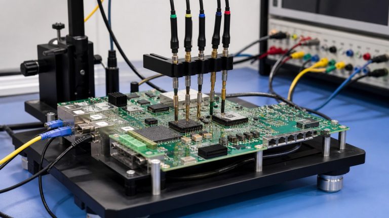
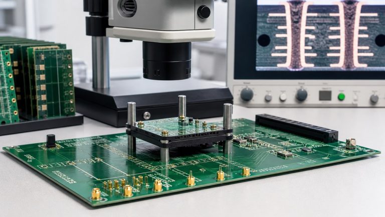
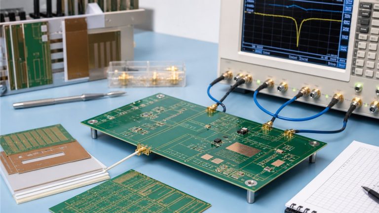
We review RF PCB designs against the material, stack-up, copper, geometry, vias, launches, finish and mechanical conditions that will be used in production. Our engineers resolve manufacturing questions before CAM release while preserving the customer’s circuit design and RF performance authority.
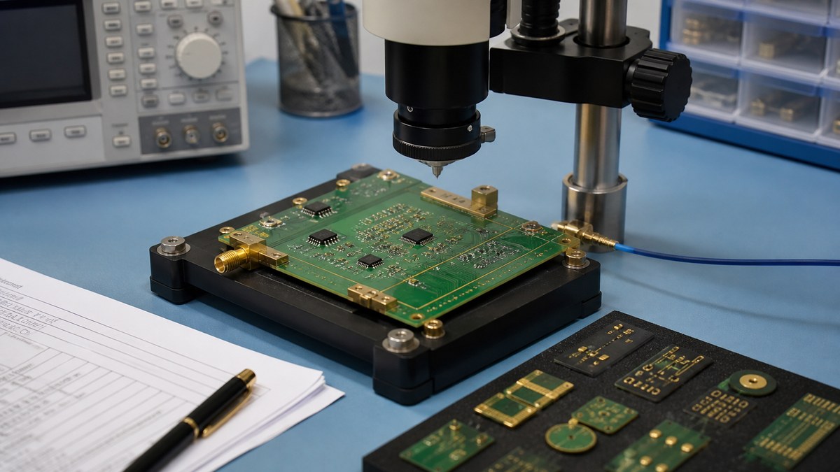
You receive an approved construction, DFM responses and the fabrication evidence planned for the lot. This prevents a material substitute, nominal stack-up or undocumented geometry compensation from changing the validated RF structure.
RF PCB Release Checklist
| Review area | Our control | Output |
|---|---|---|
| Material | Confirm grade, construction, Dk/Df basis and copper profile | Released material baseline |
| Stack-up | Control dielectrics, copper, thickness and reference planes | Approved production stack-up |
| RF geometry | Review traces, gaps, coplanar features and tolerances | Engineering response |
| Vias and launches | Control drill, registration, fences and backdrill where specified | Manufacturing and inspection plan |
| Evidence | Define coupons, impedance, dimensions and material records | Lot-linked reports |
We Need Frequency and Critical-Structure Context
We ask for operating frequency, target impedance, critical traces or regions, loss requirement, connector interfaces and any RF test responsibility. These inputs tell us which physical details need special control.
We do not infer complete RF performance from the material name. The customer’s validated design remains the electrical authority.
Material Requirements Include More Than Dk
We review Dk and Df with frequency and test method, copper roughness, resin or glass construction, thickness tolerance, thermal behavior and availability. An equivalent rule must define which differences are acceptable.
Proposed material changes receive electrical, mechanical and process review before customer approval.
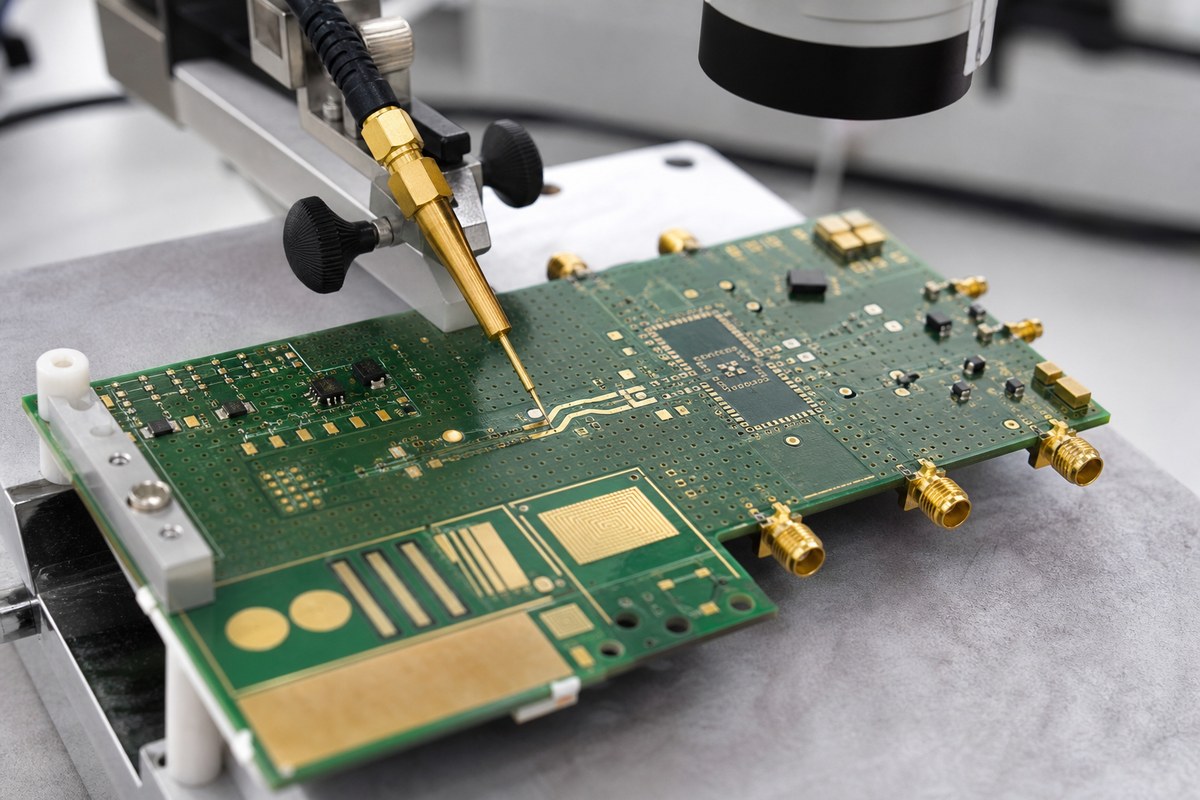
The Stack-Up and Image Data Must Agree
We compare layer functions, dielectrics, copper, finished thickness, reference planes and routed geometry. An RF trace referenced to the wrong plane cannot be fixed by an impedance coupon.
The final production stack-up becomes the basis for CAM, drilling, geometry modelling and evidence.
We Review RF Geometry Against Process Capability
Controlled traces, coplanar gaps, ground clearances, solder-mask condition and copper thickness are checked together. Fine gaps may conflict with copper weight or etching tolerance.
Any proposed manufacturing compensation is returned for approval and preserved with the released revision.
Connector Launches Need Electrical and Mechanical Context
We check footprint, board edge, reference planes, ground vias, dimensions, mounting holes and assembly access around RF connectors. The launch can be affected by both copper geometry and mechanical location.
Critical dimensions and registration can enter the inspection plan where required.
Via Fences and Transitions Need Clear Drill Data
We review via diameter, pitch, annular ring, antipad, layer transition and backdrill requirement. Dense fences still need manufacturable clearance and registration.
Structural inspection verifies selected manufactured features. RF performance testing remains a separate scope unless defined in the order.
Surface Finish and Exposed RF Features Are Controlled
We review surface-finish requirement, exposed copper areas, solder-mask openings, edge plating and contact regions. Finish affects solderability, geometry and RF interfaces differently.
The approved finish and coverage remain part of the released fabrication package.
Production Evidence Has a Defined Meaning
Impedance coupons, dimensional inspection, material identity and structural reports prove specific fabrication conditions. They do not automatically prove insertion loss, antenna performance or complete RF system behavior.
We state what each record covers so your team can combine manufacturing evidence with the correct product-level validation.
Why RF Customers Use Our DFM Review
We keep material, construction, RF geometry, vias and evidence connected before production. Your engineers can approve the real build rather than discovering fabricator assumptions after boards arrive.
This improves repeatability while keeping electrical design decisions under customer control.
Send Your RF PCB for DFM Review
Send product files, stack-up, fabrication drawing, material, frequency, impedance, loss requirement, critical structures, via and backdrill details, connector data, finish, quantities and report needs to sales@ebestpcba.com.
We will return the proposed construction, DFM questions and evidence plan.
What to Send Us Before RF Fabrication Release
Send the final RF material callout, stack-up, impedance table, copper profile requirement, controlled geometry, via and launch details, finish, mechanical data and coupon or report expectations. We will return manufacturing questions against those files. Your RF engineer retains electrical approval while we control the released fabrication route and applicable production evidence.