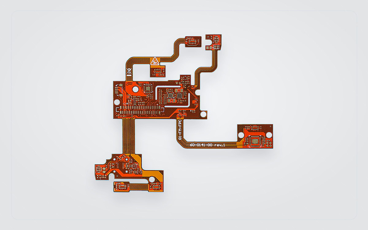
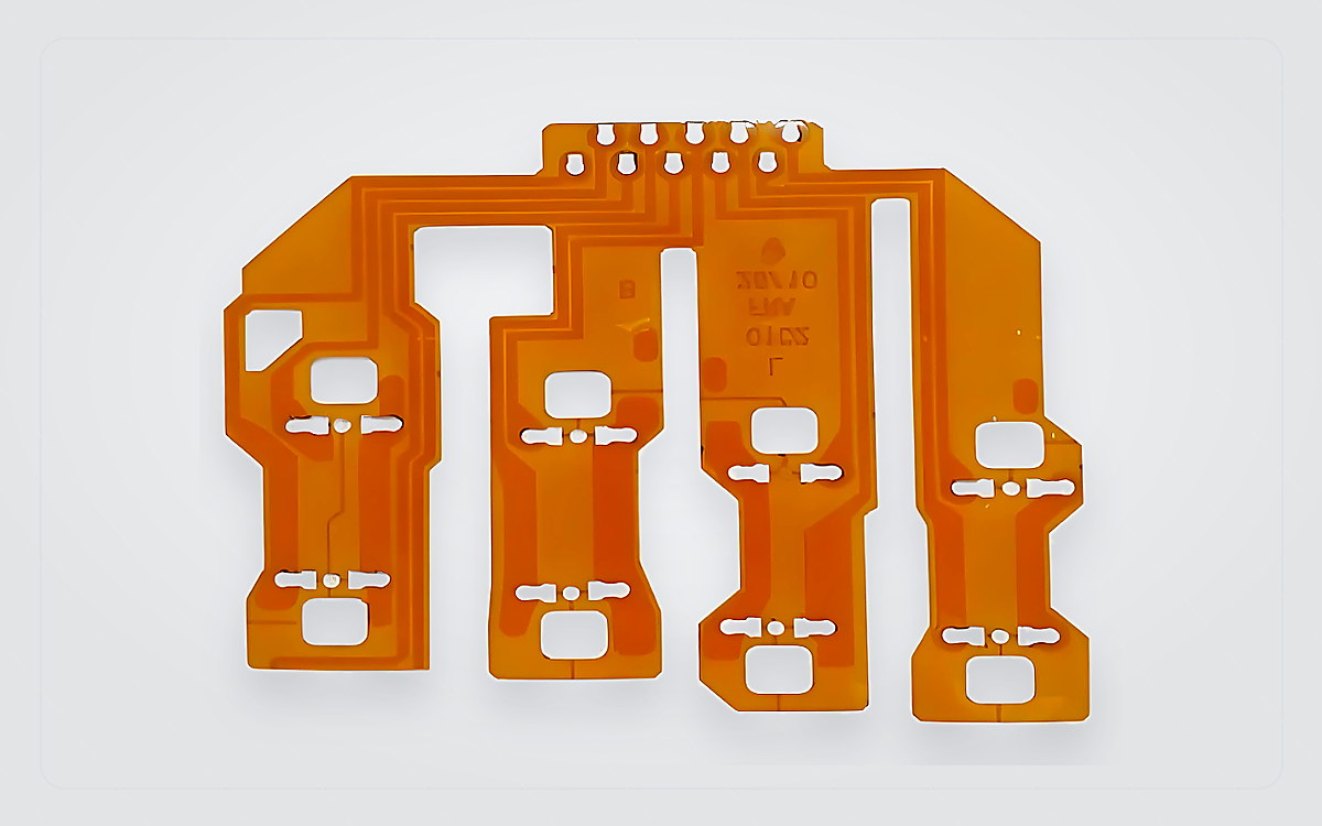
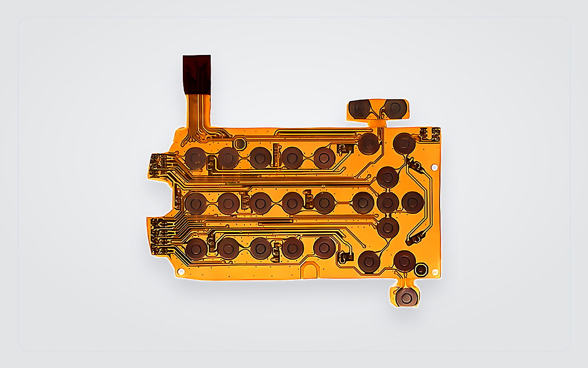
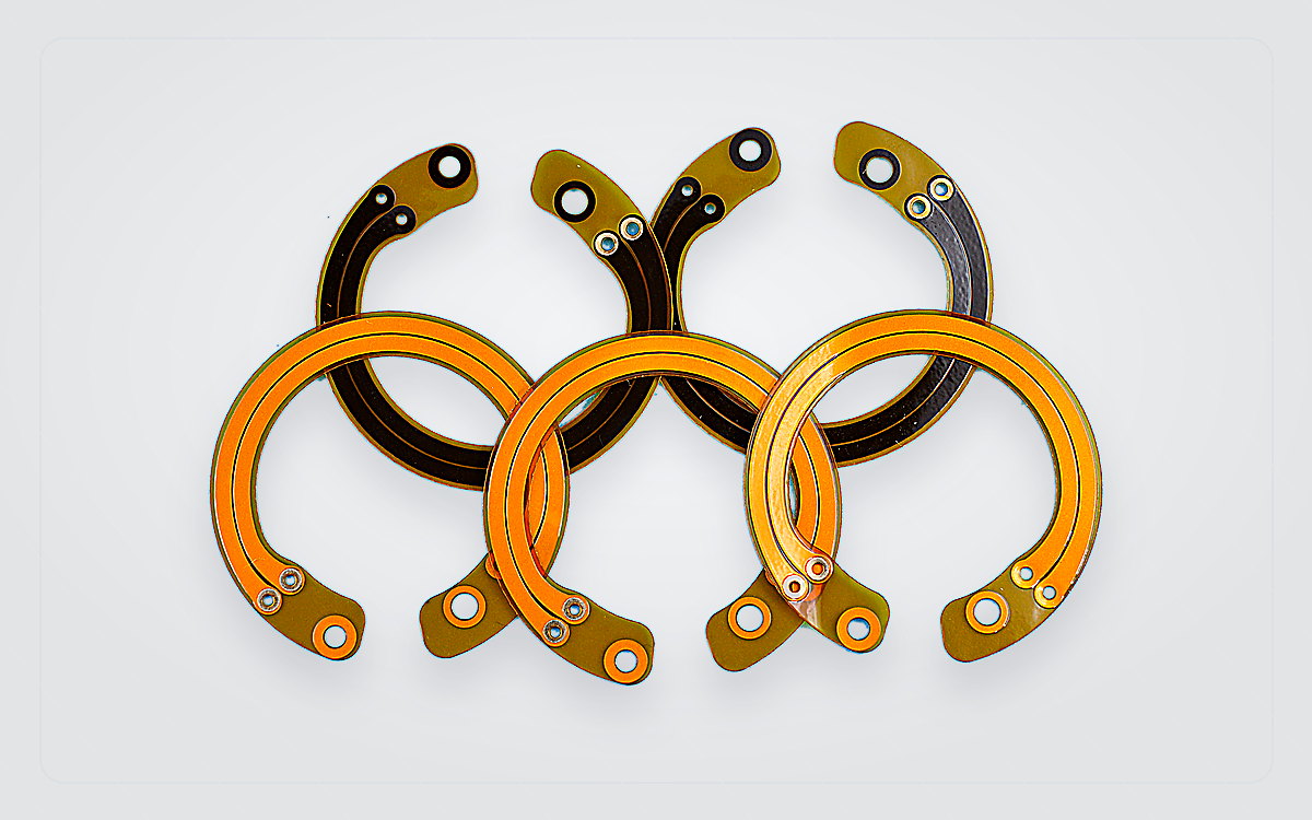
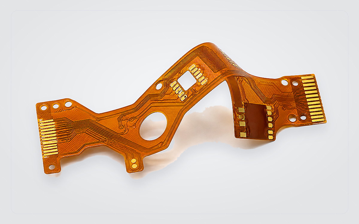
Single-Sided FPC
One conductive layer for simpler routing and lightweight interconnects.
- Review
- Bend zone, coverlay opening, stiffener and contact finish
- Fit
- Simple static or movement-sensitive interconnects
EBest PCBA manufactures single-sided, double-sided and multilayer flexible circuits for compact assemblies. We match the polyimide stack, copper, coverlay, stiffeners and contact finish to your routing and bend requirements.
We aim to provide an initial response within 12 hours. Final stack-up, bend suitability, pricing and lead time are confirmed from your project files.

Use these references to compare your design. Final limits depend on the complete flex stack, local reinforcement and bend conditions.
| Capability | Standard Process | Special Process / Conditions |
|---|---|---|
| Layer count | 1–4 layers | 5–6 layers on selected production routes; 7–8 layers subject to stack-up and process review. |
| Finished flex thickness | 0.06–0.60 mm | Coverlay, adhesive, PSA and local stiffener thickness are confirmed for each region. |
| Finished circuit size | Minimum: 5 × 10 mm | Maximum sizes vary by production route: 240 × 780 mm or 240 × 1100 mm. Selected long-board builds up to 240 × 1200 mm require review. |
| Adhesive polyimide core | PI: 0.5, 1 and 2 mil; copper: 0.33, 0.5 and 1 oz | Material grade, copper type and bend requirements are confirmed with the stack-up. |
| Adhesiveless polyimide core | PI: 0.5, 1, 2 and 3 mil; copper: 0.33, 0.5, 1 and 2 oz | Other material grades and thicknesses are subject to availability and construction review. |
| Inner-layer line / space — 18 μm finished copper | 3 / 3 mil before compensation | Special process: 2.5 / 2.5 mil; localized 2 / 2 mil features subject to engineering review. |
| Inner-layer line / space — 35 μm finished copper | 4 / 4 mil before compensation | Special process: 3.5 / 3.5 mil; final geometry reviewed with the copper and stack-up. |
| Inner-layer line / space — 70 μm finished copper | 6 / 8 mil before compensation | Special process: 5.5 / 7 mil; final geometry reviewed with the copper and stack-up. |
| Controlled impedance | ±10% | Applies to the approved stack-up, impedance targets, test method and acceptance requirements. |
| Thermosetting adhesive | 25 μm | 10 μm and 40 μm options subject to material availability and construction review. |
| PI stiffener thickness | 3, 5, 7 and 9 mil | Other thicknesses subject to availability; connector and assembly interfaces are confirmed by drawing. |
| Coverlay | Shengyi SF305C; Taiflex FHK; DuPont FR series | Grade, film / adhesive thickness and openings selected for the construction; availability confirmed before production. |
| Pressure-sensitive adhesive / mounting tape | 3M and tesa options | Examples include 3M 9077 and 467MP; tesa 8853 and 88054. Grade, thickness and application requirements are confirmed by project. |
| Electrical test pad spacing | 4–5 mil minimum | Special process: 4 mil; test access and method confirmed for the design. |
| Surface finish | ENIG, plated gold, OSP and electroplated tin | ENEPIG available through selected special-process routes, subject to project review. |
| Silkscreen character height | 0.8 mm minimum after compensation | Special process: 0.7 mm minimum after compensation. |
| Silkscreen line width | 0.127 mm minimum | Special process: 0.11 mm minimum. |

Choose the FPC structure from the available space, conductor access, bend requirements, connector locations and assembly method.

One conductive layer for simpler routing and lightweight interconnects.

Two conductive layers, with interconnection defined by the design.

One conductive layer with selected contacts accessible from both sides.

Multiple conductive layers with bend zones and local flexibility defined in the stack-up.

We select polyimide, adhesive system, rolled-annealed or electrodeposited copper, coverlay and stiffeners against your construction and use conditions. Specify bend direction, radius, angle, motion frequency and target cycles for moving interconnects.
Adhesive and adhesiveless systems selected against finished thickness and dimensional behavior.
Choose the copper type and grain direction for either static or repeated bending.
Check coverlay alignment, adhesive flow, and exposed pads before production.
PI, FR4, steel, aluminum and PSA choices tied to connector and installation interfaces.
Static flex is formed during installation and normally remains in position.
Dynamic flex moves during service and needs a construction and qualification plan matched to the movement and environment.
We check bend-zone routing, coverlay openings, stiffener transitions, vias, impedance regions and panel handling against your drawing. The review identifies the affected location, required clarification and proposed change before production.
Checks trace direction, abrupt width changes, corners and feature placement through the flexible region.
Reviews support edges, overlap, adhesive and stress transfer around contacts or mounted components.
Confirms pad exposure, registration allowance and coverlay interaction with fine traces and connector areas.
Keep vias and plated holes out of repeated bend areas. Add support where needed.
Aligns copper, dielectric thickness, trace geometry and reference structure with the target impedance.
Accounts for tooling, carrier support, assembly handling and the final separation method.
Production follows your approved data and flex stack. Electrical testing and final inspection are agreed for the build and volume. Dynamic bend qualification is defined separately, with movement, environment and acceptance criteria.
Approve fabrication data, the flex stack, bend zones and tolerances.
Prepare the selected polyimide, copper, adhesive and reinforcement materials.
Form circuits and interconnections against the approved design.
Laminate coverlay and apply reinforcement, controlling openings and registration.
Complete contacts, plating, stiffeners and final outline.
Complete electrical testing and agreed dimensional and visual inspection.
Match your routing, connector and movement requirements to the flexible circuit constructions below.

Routing and the flex stack matched to defined movement and cycle requirements.

Denser routing with controlled stack thickness, interconnections and selected bend areas.

Reinforced connector or component areas with coverlay openings and contact finish defined.
Material, cleanliness, testing, and traceability needs depend on the product and where it will be used.

Compact internal links for sensing, display or control assemblies.

Flexible connections for compact sensors, lighting and controls.

Interconnects shaped around the assembly envelope and defined motion.

Lightweight links between separated electronic modules.
Send your available fabrication data and a drawing of how the circuit fits and bends. We will confirm missing information, the proposed construction and the quotation scope.
Send the design files, available space, and movement requirements. We will check the details and reply with the next step.