
C553 — Too Close to Board Edge
The chip was 2.51 mm from the board outline against a 3.0 mm process limit.
Category: Component LayoutRisk: Depanel and handling stressAction: Review position against edge limit
DFM checks your PCB design for manufacturability before fabrication. You receive a clear report showing identified risks, affected areas, and recommended corrections so potential production issues can be addressed early.
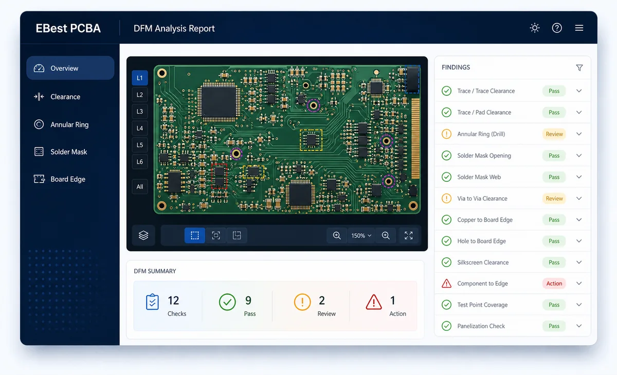
Most checks passed, but the DFM report still identified several manufacturability risks before production. Each finding was tied to a specific component or design rule, making it easier to correct the issue before fabrication and assembly.
| Board | 12-layer control board, 2.296 mm thickness |
|---|---|
| Dimensions | 254 × 406 mm |
| Assembly | 304 SMD parts and 41 through-hole parts |
| BGA details | Four BGAs, 0.5 mm minimum BGA pitch |
| Data check | 100% part-number and reference-designator match before review |
| Report identity | PCB-009238, anonymized for public display |

The DFM report identifies the exact component or location involved, explains the risk, and provides a recommended correction so your design team can update the source files before production.
The chip was 2.51 mm from the board outline against a 3.0 mm process limit.
The LFPAK56 MOSFET footprint did not fully support the pin heel.
The 2512 current-sense resistor footprint showed pin heel beyond pad.
The SOD-123 diode footprint showed a small but documented toe overrun.
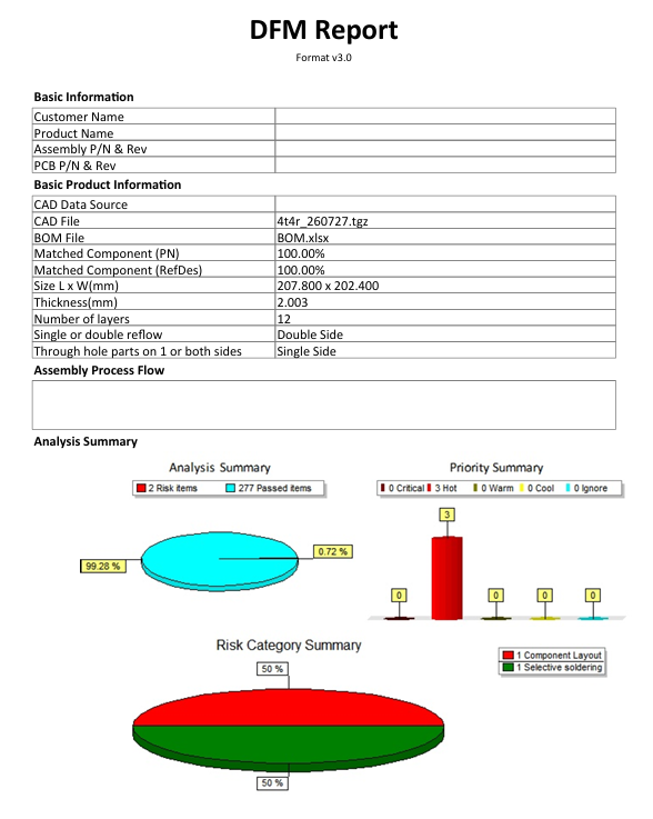
Each finding identifies the affected location, the design risk, and the recommended correction, helping your team update the source files with less back-and-forth.
CAD DRC checks the rules defined in your design tool. A DFM review goes further by checking the design against actual fabrication and assembly conditions, then showing where risks occur and how they can be corrected before production.
Checks rules configured in the CAD tool
Checks whether those rules also meet manufacturing requirements
Usually not based on factory process capability
Reviews trace, spacing, hole, pad, solder mask, assembly and other process limits
Shows the violated design rule
Identifies the affected component, pad, trace or board area
Gives a rule warning or pass/fail result
Provides the risk, measured value and recommended correction

The report is intended for practical design decisions. Questions are connected with PCB fabrication, PCBA assembly, inspection and the requested production route when those conditions affect the board.
Typical boards may be reviewed within 24 hours. Dense, incomplete or unusually large projects receive a confirmed schedule after input checking.
Request a mutual NDA before sending Gerber, ODB++, BOM or drawings.
Gerber or ODB++ plus a BOM with manufacturer part numbers can start the review.
Missing or conflicting information is identified before the review proceeds.
PCB, assembly and test-readiness conditions are checked against the project.
Findings, evidence and recommended corrections are sent back for action.
Send Gerber or ODB++, BOM, stack-up and assembly drawings. Receive a report that names the issue, location, measured value, risk and correction direction.