
Skip to content
Home / Capabilities / Testing & Inspection
Inspection Coverage and Records

PCBA Testing & Inspection Equipment

Match each PCBA risk with the appropriate SPI, AOI, X-ray, or project-defined test method. EBest PCBA confirms inspection coverage, acceptance criteria, and required records from your project files before quotation.

3D SPIPaste control3D AOIVisible defectsX-rayHidden jointsICT / FCTProject-defined
Representative inspection contextEngineer using X-ray inspection equipment to examine hidden PCBA solder joints
X-ray inspection of hidden solder-joint conditions based on the agreed inspection plan.
Inspection Method Selection

Match the Inspection Method to the Failure Risk

No single inspection method covers every defect. Start with the failure risk, then define the inspection method, required record, and acceptance criteria before production.

Inspection Risk / RequirementPrimary methodTypical evidenceConfirm Before Quotation
Paste volume, area, offset or bridging3D SPIMeasurement result and flagged locationPaste limits, control plan and record requirement
Missing, wrong, shifted or visibly defective components3D AOIReference designator, image and dispositionApproved BOM, centroid data and component library
BGA, QFN and other hidden solder jointsX-RAYInspection image and identified conditionPackage scope, void criteria, sampling and report delivery
First-board component value and reference matchFAIFirst-article verification recordBOM revision, approved alternates, and approved assembly data
Open, short or component-level electrical checksICT / FLYING PROBEProject-defined electrical test resultTest access, coverage, fixture and ownership
Product behavior, interfaces and operating limitsFCTProject-defined functional test resultFirmware, fixture, procedure, limits and golden sample
Published equipment references

PCBA Inspection Equipment and Typical Uses

Equipment selection depends on the package, defect type, and records required for the project. The specifications below are reference values; final equipment selection is confirmed from the board and assembly requirements.

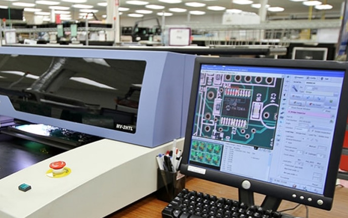
3D AOI inspection equipment and PCBA inspection interface
Paste and visible-joint control

3D SPI & 3D AOI

SPI checks solder-paste conditions before placement; AOI evaluates visible component and solder-joint conditions after assembly.

  • SPI S8080: minimum 01005 pad reference
  • SPI board window: up to 460 × 500 mm
  • AOI A51OD: 12 MP, five-camera 360° 3D imaging
  • AOI board window: up to 460 × 590 mm

X-ray inspection system for hidden PCBA solder joints
Hidden solder-joint review

AX8200 X-ray

Used where visible inspection cannot fully evaluate hidden interconnects, including BGA and other bottom-terminated packages.

  • Resolution reference: 110 LP/cm
  • System magnification: up to 600×
  • Inspection window: up to 435 × 385 mm
  • Review: bridge, void, shift and solder conditions
Operator using JCX first-article verification equipment for SMT inspection
First-board verification

JCX830 First Article

Supports component-value and first-board verification before the build moves into further production.

  • Reference error: 0.05%
  • Component checks: resistor and capacitor values
  • Output: automatic inspection report
  • Required input: approved BOM and reference data
Engineer performing project-defined functional testing on an electronic assembly
Electrical and functional testing

ICT / Flying Probe / FCT

Electrical and functional tests are configured around project access, test coverage, fixtures, software, firmware and acceptance limits.

  • Coverage: confirmed for each project
  • Confirm: fixture and software ownership
  • Define: limits, procedure and golden sample
  • Output: test results and disposition record, as required
Important: the image may show representative inspection or verification context rather than the exact published equipment model. Model, availability, program, sampling and reporting requirements are confirmed during the engineering review.
Inspection Stages

Place Inspection at the Right Stage of Production

The inspection plan can include incoming inspection, SPI, first-article verification, AOI, X-ray, electrical or functional testing, and final inspection. Not every project requires every step.

01IQC

Material, package and incoming-document checks.

023D SPI

Check solder paste before component placement.

03First Article

BOM, reference and first-board verification.

043D AOI

Visible placement and solder conditions reviewed.

05X-ray

Hidden joints reviewed where package risk requires it.

06ICT / FCT

Project-defined electrical or functional verification.

07FQC / OQC

Complete final inspection and the required outgoing records.

Inspection Records Before Shipment

Define the Inspection Records You Need

Equipment alone does not define what inspection records will be retained or delivered. Confirm report fields, image requirements, sampling rules, acceptance limits, and disposition requirements before quotation.

Inspection Report StructurePREVIEW — NOT A CUSTOMER REPORT
Lot / SNTraceability identity
MethodSPI, AOI, X-ray or test
RevisionApproved data set
U15 / BGAHidden-joint image reviewPASS
R108Placement / value correlationREVIEW
J4Visible solder-joint conditionPASS
FCT-01Project-defined functional limitPASS

A useful record answers four questions

This preview shows the structure that should be agreed. It does not claim a customer result or guarantee that every project receives every record.

  • Which board, lot, serial number and revision was inspected?
  • Which method and acceptance rule were applied?
  • Where was the exception and how was it dispositioned?
  • Which images, results or certificates must be delivered?
Representative project profiles

Start with the Product Risk, Then Build the Control Plan

These are planning examples, not customer case studies. The actual inspection plan depends on the approved files, package risks, and acceptance requirements.

Engineering team reviewing PCB layout and inspection planning requirementsRepresentative engineering review for PCB layout, inspection planning and project requirements.
01

High-density NPI with BGA or QFN

Prioritize paste control, first-article verification, AOI and a defined X-ray scope. Confirm void criteria, image retention, and first-build acceptance requirements.

02

Mixed-technology industrial PCBA

Connect SMT and through-hole inspection with AOI, visual criteria and project-defined electrical or functional checks.

03

Repeat build with traceability requirements

Use the approved BOM and inspection plan, define lot or serial records, and document exceptions and approved changes.

Related Quality Information

Review Inspection Together With Manufacturing and Quality Controls

Inspection equipment is only one part of supplier qualification. Review manufacturing capability, assembly, quality controls, and compliance documentation together.

Prepare a quote-ready review

Send the Inputs That Define Inspection Coverage

You can start with the files already available. EBest PCBA will identify missing information and confirm what is still needed before quotation.

Gerber or ODB++ dataApproved BOM and alternatesCentroid / pick-and-place dataAssembly and panel drawingsIPC class and workmanship criteriaX-ray or void requirementsICT / FCT test specificationTraceability and report requirements

Review the Inspection Plan Before You Commit the Build

Send Gerber or ODB++, BOM, assembly data, and test requirements. EBest PCBA will confirm the proposed inspection plan, missing information, and required records before quotation.

Request an Inspection Plan Review
FAQ

PCBA Inspection Questions

Are 3D SPI and AOI used on every PCBA build?
No. The inspection plan depends on the assembly process, component packages, board design, customer standard and agreed control plan. The equipment data on this page are reference values; the quotation confirms the actual inspection coverage.
When is X-ray inspection required?
X-ray is typically considered for hidden solder joints such as BGA, QFN and other packages that cannot be fully evaluated by visible inspection. The component list, risk and acceptance criteria determine the final scope.
Can EBest PCBA provide X-ray images or inspection records?
Yes, when the required records are agreed before quotation. Report content, image retention, sampling and delivery requirements can then be included in the inspection plan.
What is the difference between ICT, flying probe and FCT?
ICT and flying probe focus on electrical networks and component-level checks, while FCT verifies product behavior against project-defined functions, interfaces and limits. Coverage depends on test access, fixtures, software and customer requirements.
Who provides the FCT fixture and test software?
Fixture ownership, test software, firmware, limits, golden samples and maintenance responsibilities are confirmed during the engineering review. These responsibilities are confirmed before quotation.
What acceptance criteria should I send?
Send the applicable IPC class, workmanship standard, package-specific void criteria, sampling plan, test limits, report requirements and any customer-controlled inspection instruction. EBest PCBA will identify missing items during review.
Can an NDA be signed before test files are shared?
Yes. Request an NDA first, then send the available Gerber or ODB++, BOM, centroid data, test specification and evidence requirements for review.