
Thermal path
Define heat density, operating environment, thermal cycling and the external heat-sink or package interface before selecting Alumina, AlN, ZTA or Si3N4.
EBest PCBA supports ceramic circuit projects with route-specific material, conductor and assembly review. Compare DPC, DBC, AMB and thick-film constructions, or discuss LTCC and HTCC requirements, then send your drawing to confirm the suitable route.
We aim to provide an initial response within 12 hours. Material, manufacturing route, inspection scope and lead time are confirmed for your project.
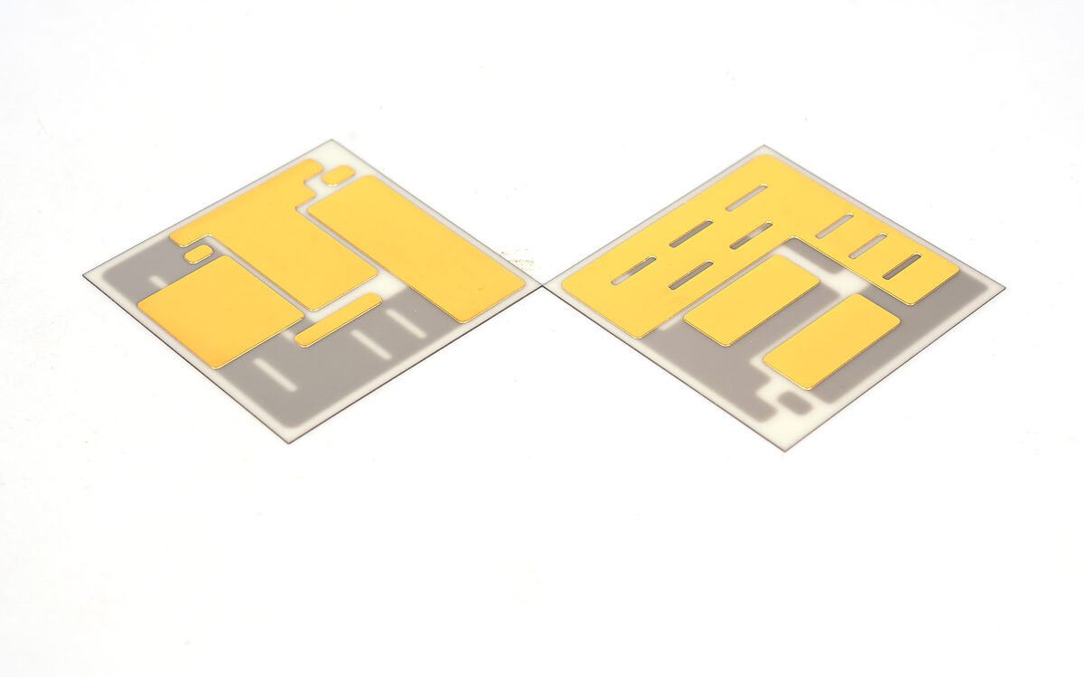
Define heat flow, electrical isolation, operating environment, attachment and bonding requirements. We review the candidate material and process together rather than selecting a substrate independently of the conductor system.
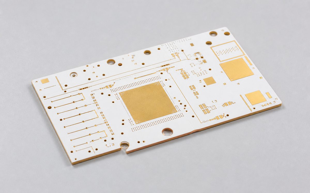
Define heat density, operating environment, thermal cycling and the external heat-sink or package interface before selecting Alumina, AlN, ZTA or Si3N4.
Confirm voltage withstand, creepage, dielectric behavior and conductor-to-edge requirements together with substrate thickness and surface condition.
Fine patterned copper, thick copper, printed conductor paste and co-fired metallization follow different DPC, DBC, AMB, Thick Film, LTCC or HTCC routes.
Soldering, wire bonding, die attach, component clearance, finish, flatness and inspection requirements must be defined before the board route is released.
Compare three process families: patterned or bonded copper (DPC, DBC and AMB), printed-and-fired thick-film conductors, and co-fired LTCC / HTCC circuits. Material compatibility and available project scope are reviewed separately for each route.
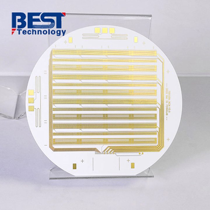
For finer copper geometry where conductor thickness, adhesion, surface finish and thermal interface are reviewed as one build.
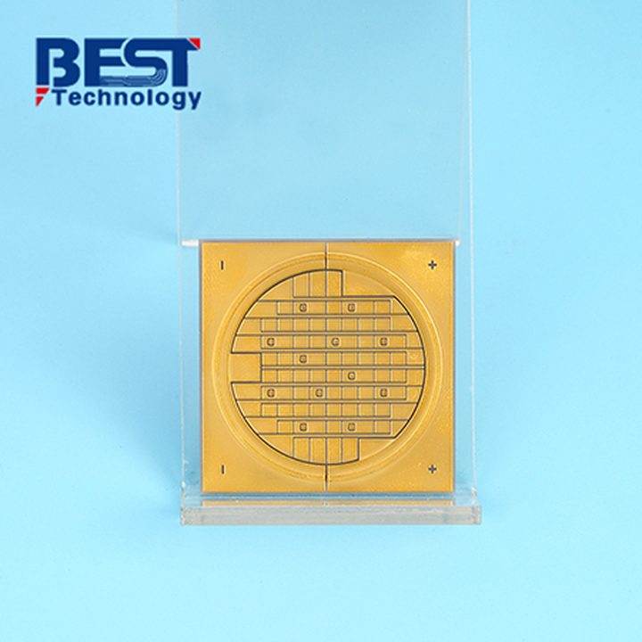
For higher-current power circuits where bonded copper, ceramic isolation, thermal cycling and module attachment control the route.
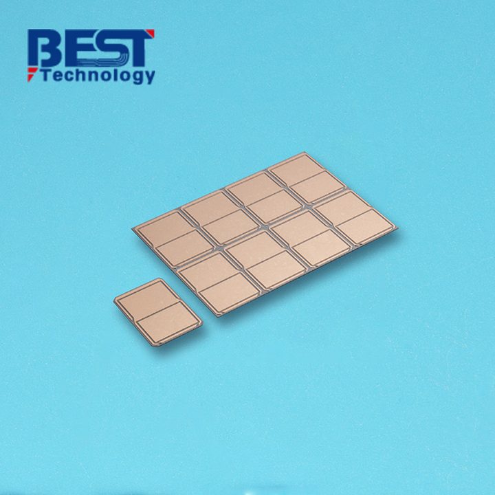
For power-module builds where higher current, cycling load, substrate selection and bonding reliability must be confirmed together.
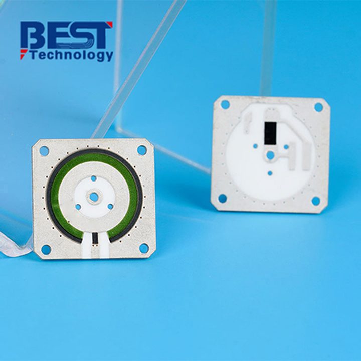
For printed paste circuits where firing profile, glaze, conductor geometry and downstream bonding or soldering must be aligned.
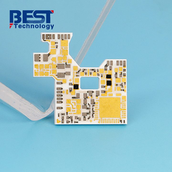
For multilayer ceramic circuits where conductor compatibility, cavities, buried structures and shrinkage control affect release.
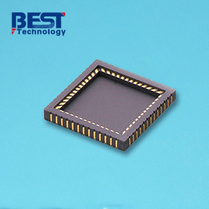
For ceramic packages where conductor system, firing route, multilayer structure and environmental reliability define the build.
The substrate, conductor system and manufacturing process must form an approved combination. The references below apply to their named routes and cannot be combined into one universal capability.
| Item / Route | Production Reference | Conditions / Special Review |
|---|---|---|
| Ceramic materials | Alumina (Al₂O₃), AlN; ZrO₂ and Si₃N₄ on supported routes | Grade, process compatibility and availability confirmed. ZTA is a separate material option requiring project review. |
| Thick Film — layers and conductors | Up to 10 layers; fired conductor thickness 5–13 μm | Paste system, firing conditions, vias and assembly interface confirmed for the construction. |
| Thick Film — panel and geometry | Maximum panel: 200 × 200 mm; line / space: 6 / 8 mil | Approximately 0.15 / 0.20 mm; geometry depends on the fired conductor and printing process. |
| Thick Film — finished thickness | 0.25–2.0 mm reference | Ceramic, fired conductors and coatings defined in the drawing. |
| DPC — layers and conductors | 2-layer reference; conductor thickness 2–200 μm | Single- or double-sided circuit arrangement, copper thickness, adhesion and hole structure confirmed. |
| DPC — panel and geometry | Maximum panel: 138 × 190 mm; line / space: 6 / 8 mil | Approximately 0.15 / 0.20 mm; minimum geometry and maximum copper thickness are not automatically compatible. |
| DPC — finished thickness | 0.25–2.0 mm reference | Approved substrate, copper and finish define the finished construction. |
| DBC — layers and copper | 2-layer reference; copper thickness 3.9–8.6 oz | Ceramic, copper bonding, balance and thermal-cycling requirements reviewed together. |
| DBC — panel and geometry | Maximum panel: 138 × 178 mm; line / space: 12 / 12 mil | Approximately 0.30 / 0.30 mm; copper thickness and bonding route confirmed. |
| DBC — finished thickness | Minimum 0.30–0.40 mm by construction; maximum 1.3 mm (1L) or 1.6 mm (2L) | Layer definition, substrate and copper inclusion confirmed on the approved stack. |
| AMB — layers and copper | 2-layer reference; copper thickness 8–22.9 oz | Active-metal bond system, ceramic, copper balance and qualification requirements agreed. |
| AMB — panel and geometry | Maximum panel: 114 × 114 mm; line / space: 20 / 20 mil | Approximately 0.50 / 0.50 mm; geometry matched to the copper and bonded construction. |
| AMB — finished thickness | 0.25–1.8 mm reference | Approved ceramic, bonding and conductor construction defines finished thickness. |
| Thick Film / DPC — substrate thickness | 0.25, 0.38, 0.50, 0.635, 0.80, 1.0, 1.25, 1.5 and 2.0 mm | Substrate options by route and material; these are not finished-board thickness limits. |
| DBC / AMB — substrate thickness | 0.25, 0.38, 0.50, 0.635, 0.76 and 1.0 mm | Material grade, bonding compatibility and complete finished thickness confirmed separately. |
| LTCC / HTCC | Project-specific route review | Layer arrangement, conductor system, vias, firing shrinkage and supply availability confirmed before quotation. |
| Surface and assembly interface | DPC / DBC / AMB: OSP, ENIG and immersion silver references; thick-film metallization selected by conductor system | Other finishes and bonding interfaces reviewed for process compatibility; soldering, die attach and wire bonding have separate requirements. |
Layer count, geometry, conductor thickness and panel dimensions belong to the selected process. The quote confirms the material, complete construction, tolerances and agreed inspection scope.
We approve the material, conductor and route before production. Processing follows the selected plating, bonded-copper, printed-and-fired or co-fired construction. Geometry, surface condition and electrical checks follow the agreed quality plan.
Gerber or ODB++, drawing, material, conductor, quantity, thermal and assembly notes are checked for missing inputs.
Substrate, thickness, conductor system and DPC, DBC, AMB, Thick Film, LTCC or HTCC route are confirmed before pricing.
Printing, plating, bonded copper or co-fired operations follow the approved construction, geometry, holes, outline and finish.
Dimensions, conductor geometry, isolation, surface condition, traceability and assembly handoff are checked before shipment.
Define conductor thickness, dimensions, flatness, edge quality, holes or vias, continuity and isolation requirements. Adhesion, thermal cycling, bonding suitability and other qualification tests are included only when agreed for the construction.
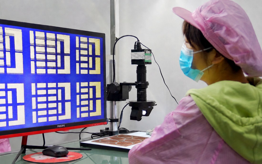
Material identification, thickness, surface condition and project-specific mechanical requirements are checked before circuit processing.
Line width, spacing, conductor or copper thickness, pads, holes, outline and edge clearance follow the released drawing and route.
Glaze, solder mask, finish, via or through-hole strategy, wire-bonding and soldering interfaces are checked for compatibility.
Continuity and isolation checks follow the agreed test plan. Thermal cycling, adhesion and other qualification tests are specified separately for the construction.
Released revision, lot information, inspection records and packaging route are aligned with the order and downstream assembly needs.
Ceramic PCBs are commonly used in applications that require efficient heat dissipation, electrical isolation, dimensional stability and reliable performance in demanding environments.

Circuit substrates for specified electronic modules and documented assembly needs.
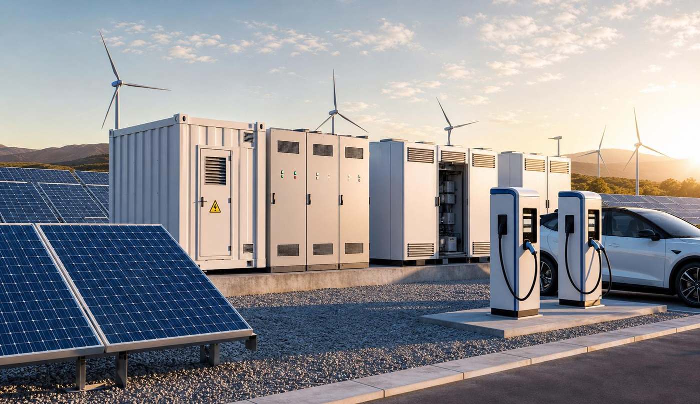
Heat flow, isolation and attachment interfaces for selected power-module constructions.
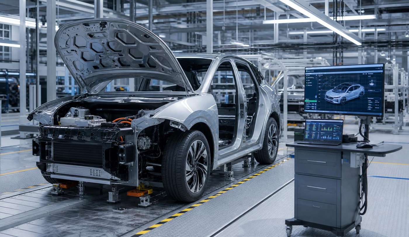
Selected power and sensing assemblies with defined cycling and traceability requirements.
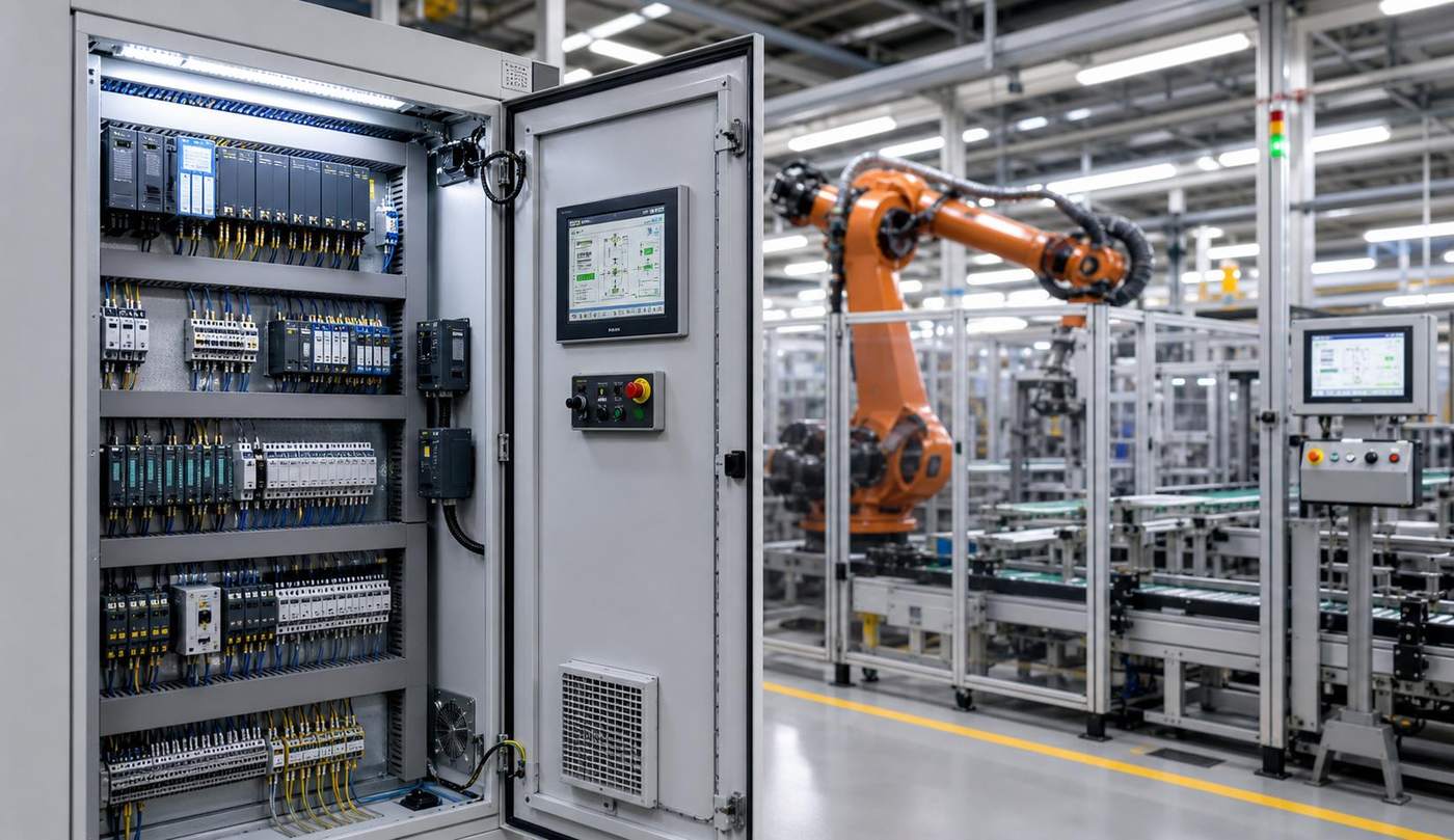
Power, sensing or control functions with defined thermal and electrical interfaces.
Send your drawing, available circuit data and quantity. If the process is not yet selected, describe the thermal, electrical and assembly requirements so we can review candidate constructions.
Share your drawing and application requirements. We will review the material, conductor and manufacturing route, then confirm the information needed for pricing and production.
These FAQs cover common questions about ceramic PCB materials, manufacturing processes, surface finishes, quotations and assembly.