Skip to content
Home / Services / PCB Fabrication
Engineering-led PCB manufacturing

PCB Fabrication Controlled From DFM to Production Release

Send your PCB data for a review of stack-up, material, impedance, panelization and production risk before quotation. FR4, flexible, rigid-flex, metal-core, ceramic and specialty routes are assessed against the actual files.

8 FacilitiesSpecialized group production300,000+ m²/moPublished group capacityUL E502832Published construction file12h ResponseInitial project check
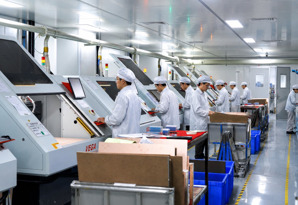
PCB manufacturing and inspectionFACTORY EVIDENCE
PCB fabrication production line with operators running manufacturing equipment
Final capability, construction and production schedule are confirmed from the released project files.
Project fit

Is EBest PCBA the Right Fabrication Route for Your Project?

Select the PCB construction from the design files, stack-up, material, copper, impedance, assembly and inspection requirements—not from the category name alone.

Engineer reviewing DFM findings and BOM optimization for PCB fabrication release
PCBA production line supporting downstream assembly after PCB fabrication.
01

PCB and PCBA under one owner

Keep board fabrication, sourcing and assembly questions inside one accountable project workflow.

02

Flex, rigid-flex or multilayer decisions

Confirm material, bend area, stack-up, drilling and impedance against a real production route.

03

Thermal, copper or size constraints

Review metal-core, ceramic, heavy-copper or long-format needs before the design becomes expensive to change.

04

Prototype moving toward repeat builds

Turn approved prototype data into controlled fabrication inputs before volume demand increases.

Capability review

PCB Fabrication Capabilities Used for Early Project Screening

These published ranges support early supplier screening. Final capability, tolerance, material availability, price and schedule are confirmed only after engineering reviews the actual files.

Board routePublished working rangeWhat engineering verifies
FR4 & Multilayer12-layer everyday productionStack-up, copper, controlled impedance ±10%, finish and panelization.
Flexible PCB1–2 layers; 75 μm trace/space; 0.20 mm minimum drillBend zone, stiffener, coverlay opening, drill and material selection.
Rigid-FlexUp to 14 layers; 0.15 mm minimum drill; thin builds to 0.42 mmRigid/flex transition, via location, thickness, fold direction and reliability risk.
Metal Core PCBAluminum-base thermal buildsThermal path, dielectric, copper, finish and assembly heat profile.
Ceramic PCBHigh-thermal and high-frequency substratesMaterial fit, metallization, tolerance, finish and operating environment.
Specialty / HDIMixed-substrate, heavy-copper and long-format builds by reviewDrill, trace/space, impedance, panel size, bow/twist and yield constraints.
Capability summary version: July 2026Project-specific limits are confirmed in the quotation after file review.

Need a limit that is not published here? Send the board data and required tolerance for a file-specific capability check.

Request capability review
PCB manufacturing cases

18 PCB Manufacturing Cases

Review manufacturing examples by PCB construction and application. Send your files to confirm material, dimensions, tolerances, inspection requirements and production schedule.

Flexible PCB Cases

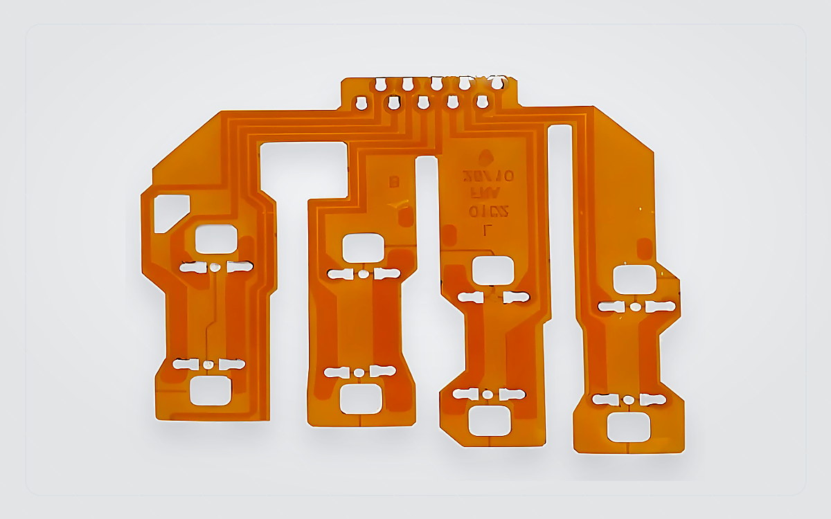
Single-sided flexible printed circuit
Flexible PCB

Single-Sided FPC

A lightweight flexible interconnect for compact assemblies, replacing discrete wiring where controlled routing and repeatable termination are needed.

Typical application: sensors, displays, compact modules and cable replacement.
Material
Polyimide with coverlay or specified protective layer
Layers
Single conductive layer
Finish
ENIG or immersion tin by termination requirement
Key review
Bend zone, stiffener, connector and outline tolerance
Release basis
Approved flat pattern and mechanical interface
Review this build
Double-sided and multilayer flexible PCB
Dense flexible interconnect

Double-Sided / Multilayer FPC

Additional routing density and interconnection for flex circuits that must carry more signals while maintaining controlled mechanical behavior.

Typical application: cameras, medical modules, wearables and compact instrumentation.
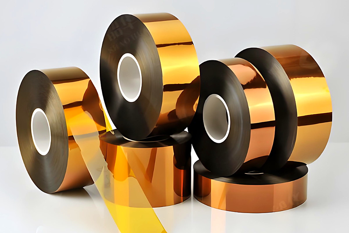
Material
Polyimide construction with adhesive or adhesiveless options
Layers
Two or more layers after bend and stack-up review
Finish
Matched to connector, soldering and storage conditions
Key review
Via placement, neutral axis, coverlay opening and stiffener
Release basis
Approved flex stack-up and bend definition
Review this build
Flexible PCB with stiffeners and dynamic bend zones
Mechanical flex design

Dynamic-Flex & Stiffener FPC

A mechanically reviewed flex route for assemblies that move, fold or require local reinforcement at connectors and component areas.

Typical application: moving heads, hinged devices, robotics and precision sensors.
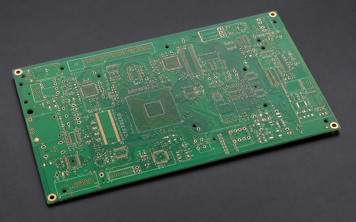
Material
Polyimide with PI, FR4 or specified local stiffener
Motion
Bend radius and cycle requirement confirmed from use case
Finish
Defined around termination and contact requirements
Key review
Dynamic zone, grain direction, transition and strain relief
Release basis
Approved mechanical envelope and bend conditions
Review this build

FR4 & Multilayer PCB Cases

Multilayer FR4 control PCB panel
FR4 & multilayer

Multilayer Control PCB

A coordinated multilayer route for control, instrumentation and communication boards where stack-up, drill structure and panel strategy affect repeatability.

Typical application: industrial controllers, instrumentation and communication backplanes.
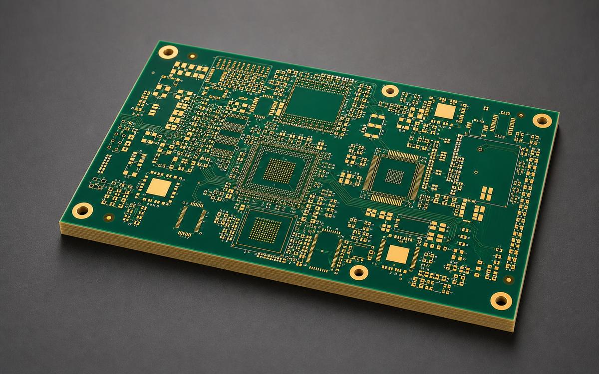
Material
FR4 laminate selected to operating and assembly conditions
Layers
12-layer routine reference; higher builds reviewed from files
Finish
ENIG, HASL or OSP according to assembly and storage needs
Key review
Stack-up, copper balance, drill map and panel utilization
Release basis
Approved fabrication data and quotation
Review this build
High Tg FR4 printed circuit board
Thermal-cycle FR4

High-Tg FR4 PCB

High-Tg laminate construction for boards exposed to demanding lead-free assembly, sustained heat or repeated thermal cycling.

Typical application: power conversion, industrial electronics and high-temperature control.
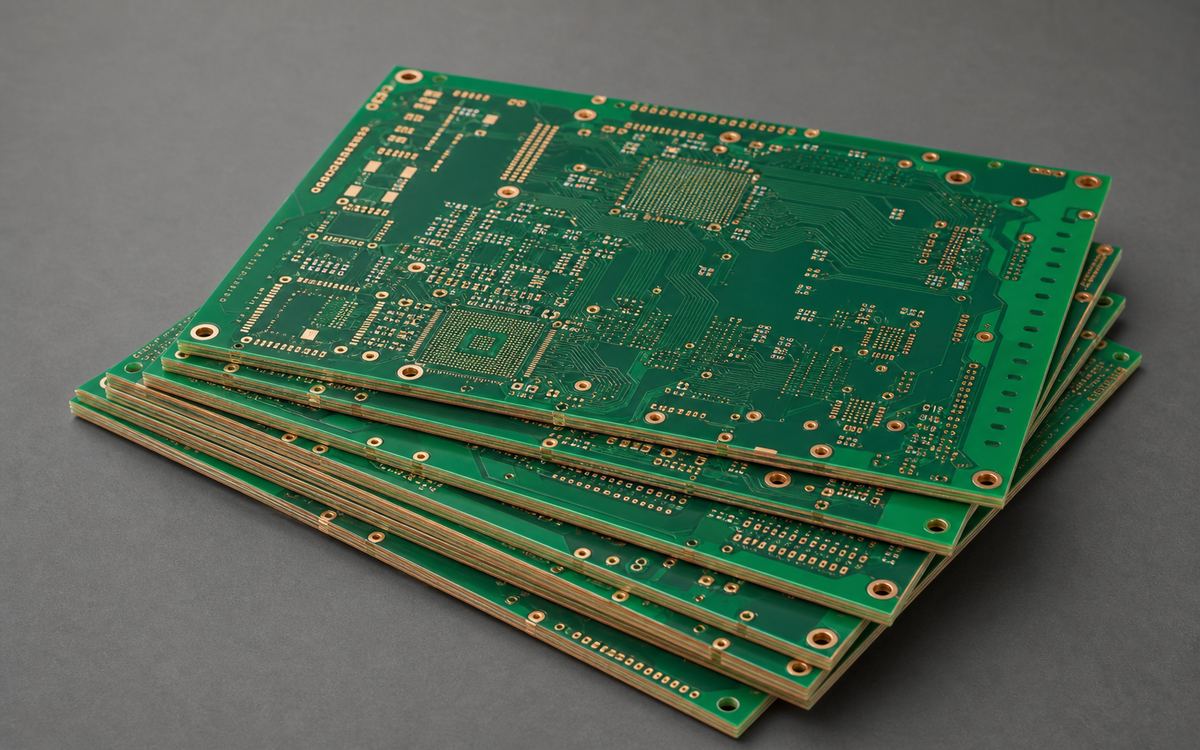
Material
High-Tg FR4 grade confirmed against project conditions
Layers
Multilayer construction by stack-up review
Finish
Selected for component, shelf-life and soldering requirements
Key review
Tg, laminate brand, CAF risk and thermal-cycle exposure
Release basis
Material approval and controlled stack-up
Review this build
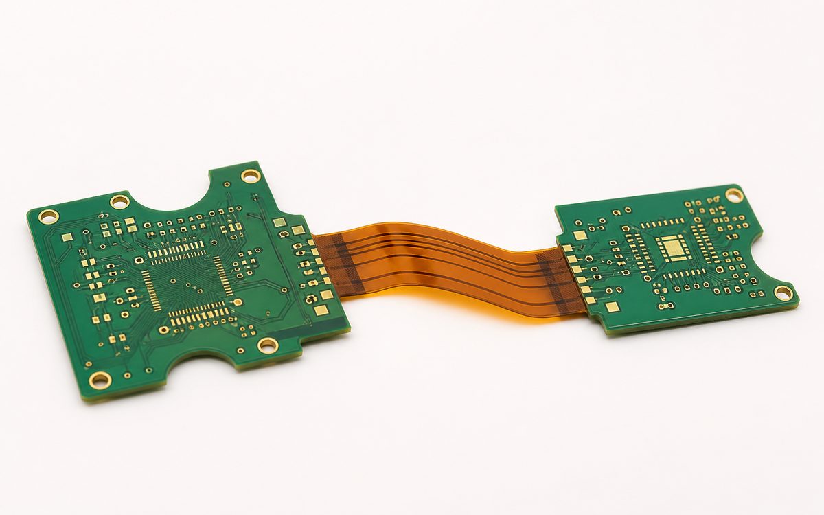
Controlled impedance multilayer PCB
Signal integrity

Controlled-Impedance PCB

A stack-up-led route for high-speed digital and RF-related nets, aligning laminate, copper geometry, reference planes and verification coupons.

Typical application: network equipment, high-speed control and data acquisition.
Material
FR4 or low-loss laminate selected after stack-up review
Impedance
±10% is a typical review target; final tolerance is quoted
Verification
Coupon and test method defined before production
Key review
Trace geometry, dielectric data, reference plane and finish
Release basis
Approved impedance table and production stack-up
Review this build

Rigid-Flex PCB Cases

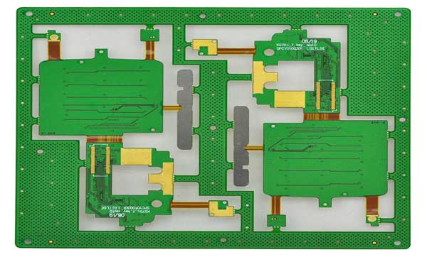
Basic rigid-flex printed circuit board
Integrated interconnect

Basic Rigid-Flex PCB

Rigid component regions joined by integrated flexible sections, reducing connectors and assembly steps inside compact products.

Typical application: compact controls, portable instruments and enclosure-constrained electronics.
Material
FR4 rigid sections with polyimide flex construction
Layers
Defined by routing density and mechanical interface
Finish
Selected for assembly and exposed contact areas
Key review
Transition, bend zone, coverlay and component keep-out
Release basis
Approved stack-up and mechanical drawing
Review this build
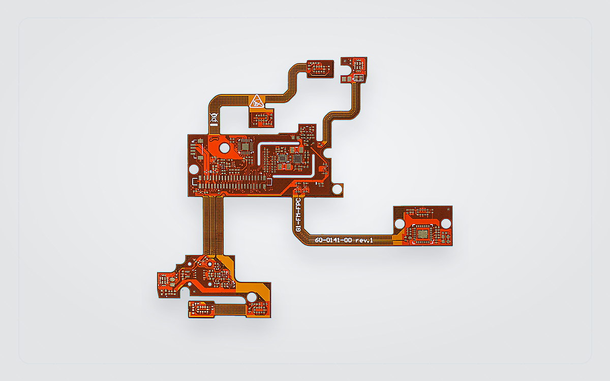
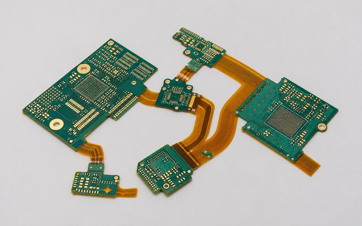
Multilayer rigid-flex PCB construction
Complex rigid-flex

Multilayer Rigid-Flex PCB

A higher-density construction coordinating multilayer rigid regions, flex layers, plated holes and sequential assembly constraints.

Typical application: avionics modules, medical equipment and dense industrial assemblies.
Material
FR4 and polyimide system qualified as one stack-up
Layers
Up to the published category range after file review
Construction
Layer transition and rigidization are project-specific
Key review
Via structure, copper balance, bookbinding and bend geometry
Release basis
Controlled stack-up and fabrication notes
Review this build
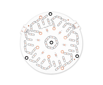
High-density rigid-flex PCB
High-density integration

High-Density Rigid-Flex PCB

An engineering-led route for compact rigid-flex designs that may require fine geometry, microvias or dense interconnect transitions.

Typical application: imaging, miniature communications and advanced portable systems.
Material
Low-profile copper and qualified rigid/flex laminate system
Interconnect
HDI and microvia structure confirmed after data review
Finish
Matched to fine-pitch assembly and contact needs
Key review
Via-in-pad, sequential lamination, registration and flex escape
Release basis
Approved HDI stack-up and drill sequence
Review this build

Metal Core PCB Cases

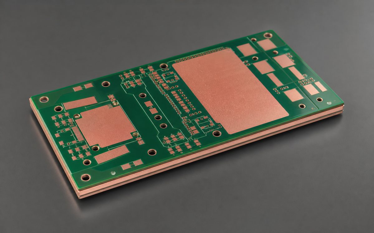
Aluminum core PCB for thermal management
Metal core PCB

Aluminum PCB

A cost-conscious thermal route using an aluminum base to move heat from LEDs, power devices and compact control assemblies.

Typical application: LED lighting, power supplies, chargers and motor control.
Base
Aluminum alloy selected to mechanical and thermal needs
Dielectric
Thickness and thermal class confirmed in quotation
Copper
Selected from current and etching requirements
Key review
Isolation, flatness, mounting holes and heat path
Release basis
Approved material stack and mechanical drawing
Review this build
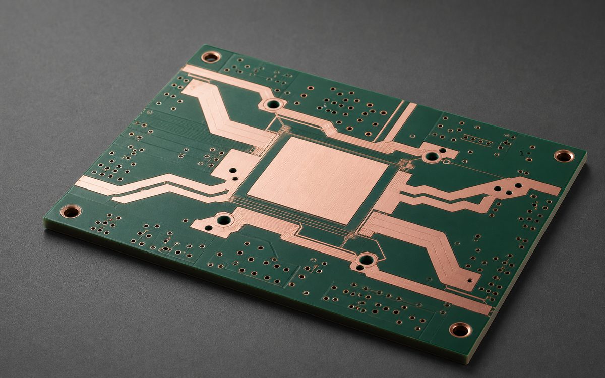
Copper-core printed circuit board
Higher thermal mass

Copper-Core PCB

A copper-base construction considered where heat spreading, local thermal load or mechanical mass exceeds the intended aluminum route.

Typical application: high-power lighting, converters and concentrated heat-source modules.
Base
Copper base or core structure after manufacturability review
Dielectric
Electrical isolation and thermal path jointly specified
Finish
Chosen for assembly and exposed copper protection
Key review
Machining, plated features, flatness and heat-source location
Release basis
Approved thermal and mechanical construction
Review this build
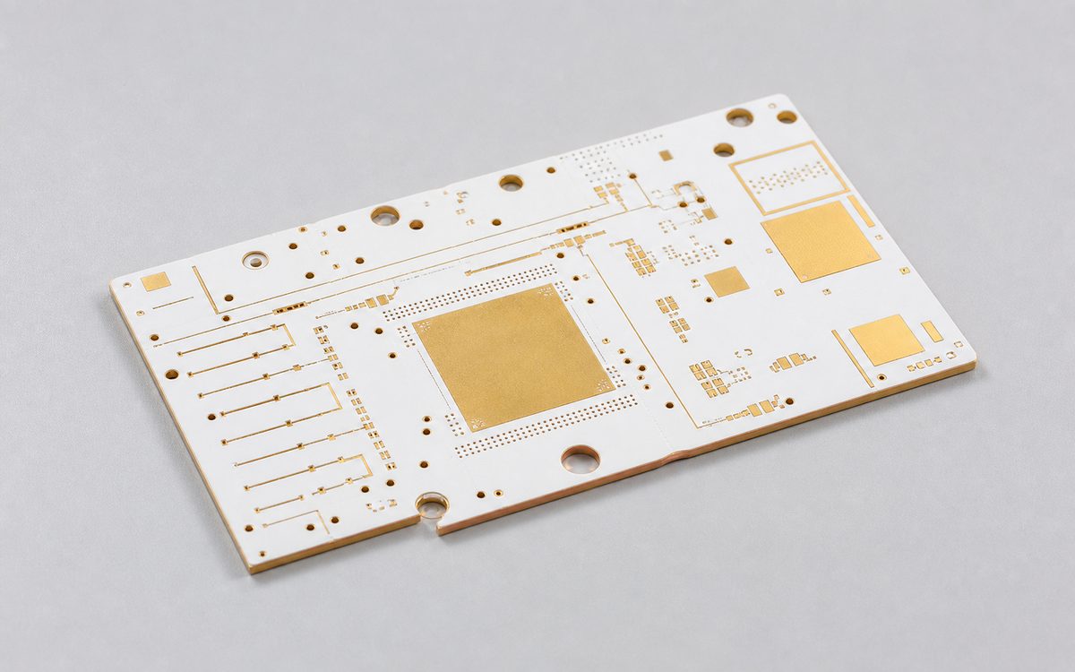
Copper inlay and direct thermal path PCB
Localized heat transfer

SinkPAD / Copper-Inlay PCB

A specialized route that places a direct or concentrated copper heat path beneath selected devices instead of treating the full board uniformly.

Typical application: high-power LEDs, laser drivers and localized power stages.
Structure
Copper inlay or direct thermal path defined from device geometry
Isolation
Electrical boundary confirmed around the heat-transfer feature
Assembly
Pad coplanarity and solder interface reviewed
Key review
Inlay tolerance, routing, machining and inspection access
Release basis
Approved cross-section and device footprint
Review this build

Ceramic PCB Cases

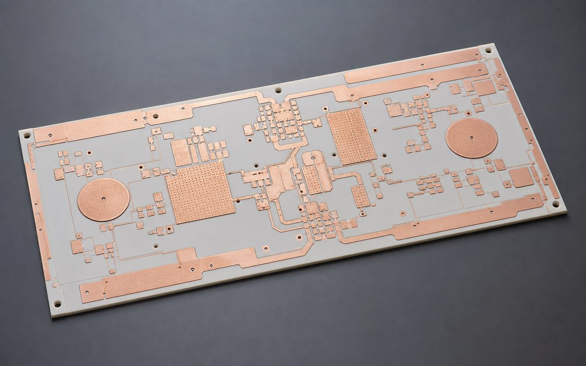
Alumina ceramic printed circuit board
Ceramic substrate

Alumina Al2O3 PCB

A stable ceramic substrate route balancing electrical insulation, dimensional stability and thermal transfer for demanding electronics.

Typical application: sensors, power modules, instrumentation and hybrid circuits.
Substrate
Alumina grade and thickness confirmed from project need
Metallization
Selected for conductor, bonding and assembly process
Finish
Specified around soldering, wire bonding or contact use
Key review
Outline tolerance, vias, edge condition and attachment
Release basis
Approved material and metallization drawing
Review this build
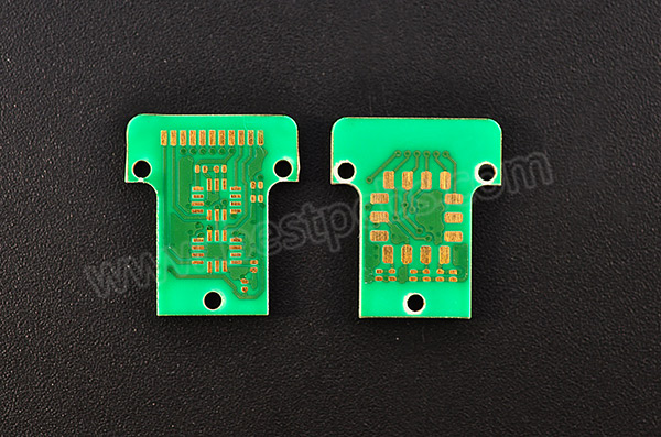
Aluminum nitride ceramic PCB
High thermal demand

Aluminum Nitride AlN PCB

Aluminum nitride may be considered when the design requires high thermal conductivity together with ceramic electrical insulation.

Typical application: high-power semiconductors, RF modules and optical systems.
Substrate
AlN grade and source confirmed before quotation release
Metallization
Process selected for current, bonding and reliability needs
Assembly
Interface material and flatness requirement reviewed
Key review
Heat source, thermal interface, outline and brittle handling
Release basis
Approved substrate and assembly conditions
Review this build
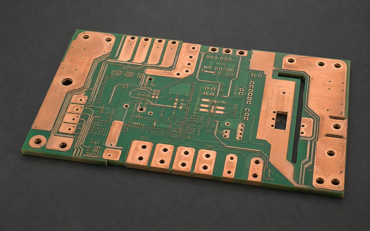
DBC and DPC ceramic circuit board
Ceramic metallization

DBC / DPC Ceramic PCB

Process-specific ceramic constructions for thicker copper, fine metallization or specialized power and packaging requirements.

Typical application: power modules, IGBT assemblies, RF packages and laser systems.
Process
DBC or DPC route selected from copper and geometry needs
Substrate
Ceramic type and thickness confirmed in engineering review
Finish
Defined around solder, sinter or bonding process
Key review
Copper profile, ceramic edge, warpage and joining method
Release basis
Approved cross-section and assembly process
Review this build

Specialty PCB Cases

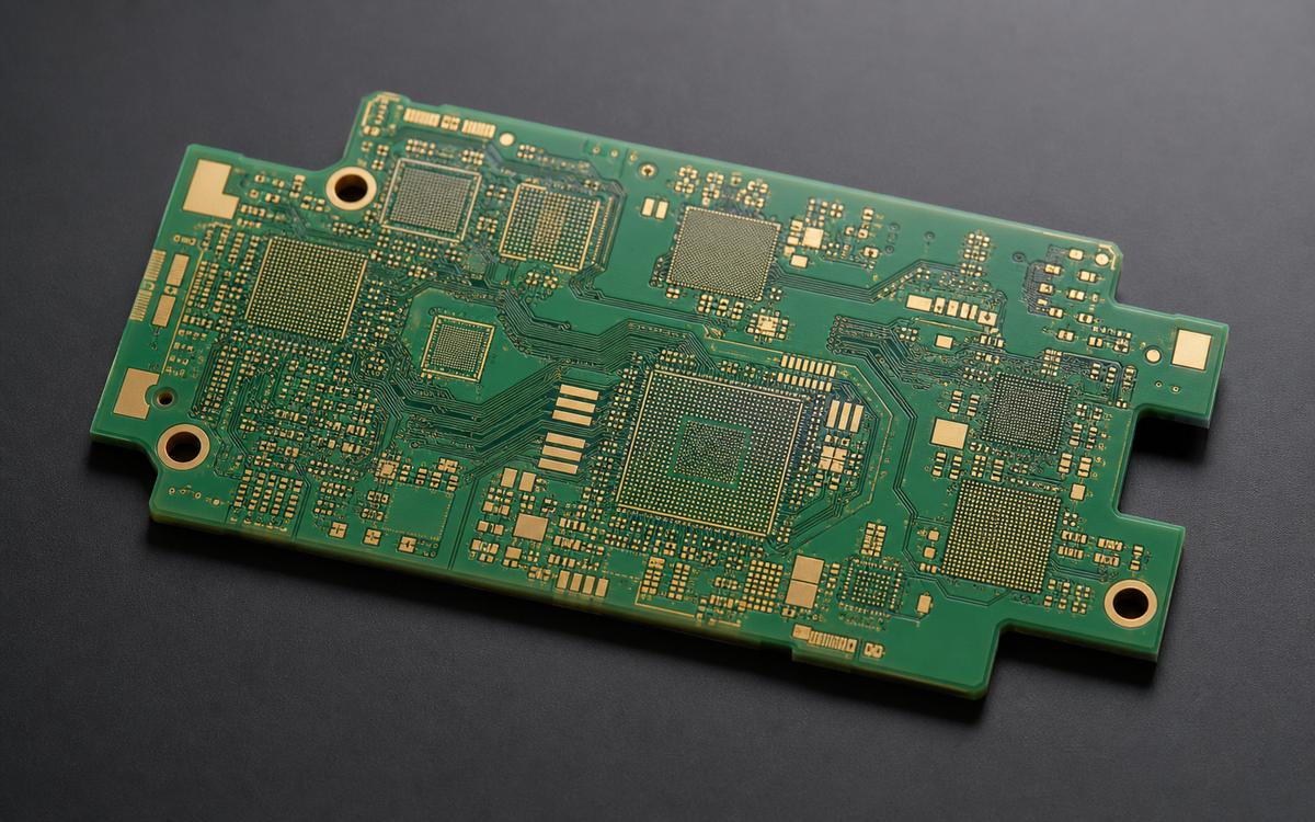
Heavy copper printed circuit board
High-current PCB

Heavy-Copper PCB

A copper-intensive route for high-current paths and thermal loading, where etching, spacing, plating and resin fill must be balanced.

Typical application: power distribution, converters, battery systems and industrial drives.
Copper
Heavy-copper construction confirmed from current and geometry
Material
Laminate and resin system selected for copper balance
Finish
Matched to assembly and exposed terminal requirements
Key review
Spacing, plated holes, copper steps, thermal relief and fill
Release basis
Approved current map and fabrication cross-section
Review this build
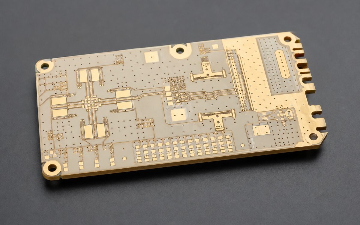
High-density interconnect HDI PCB
High-density interconnect

HDI PCB

A sequential-build route for designs using fine-pitch components, laser microvias and dense escape routing where registration and via structure drive yield.

Typical application: compact communications, medical modules and advanced embedded systems.
Interconnect
Laser microvia and HDI stack-up confirmed from source files
Layers
Sequential lamination structure by engineering review
Finish
Selected for fine-pitch assembly and storage conditions
Key review
Via type, capture pad, stacking, fill and registration
Release basis
Approved build-up and drill sequence
Review this build
Rogers and PTFE high-frequency PCB
RF & microwave PCB

Rogers / PTFE PCB

A material-controlled route for RF and microwave circuits, coordinating laminate data, copper profile, impedance, surface finish and mechanical handling.

Typical application: antennas, radar, RF front ends and high-frequency test equipment.

Material
Rogers, PTFE or low-loss laminate confirmed by part number
Stack-up
Pure or hybrid construction reviewed for compatibility
Impedance
Geometry and tolerance quoted from dielectric data
Key review
Copper profile, registration, finish, handling and test coupon
Release basis
Approved material declaration and impedance table
Review this build

Not sure which case is closest to your project? Send the Gerber/ODB++, stack-up, quantity and the constraint you cannot compromise for an engineering comparison.

Discuss a similar PCB project
Manufacturing evidence

Evidence Across Review, Inspection and Assembly Handoff

Controlled manufacturing records, inspection evidence and traceability data help protect your product quality and connect every PCBA build to its approved revision, materials, production process and release results.


Operator scanning PCB assemblies with traceability records displayed
Inspection equipment used to connect CAM data with measurable manufacturing checks.
Cross-functional engineering team reviewing PCB layout and manufacturing data
Engineering review of PCB layout, stack-up and manufacturing requirements.
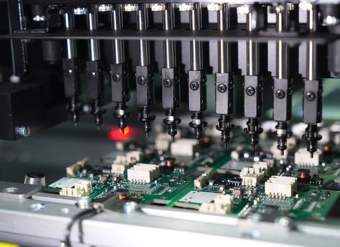
Automated placement equipment assembling components on printed circuit boards
Downstream PCBA handoff when the project continues from bare board into assembly.
UL E502832Published board construction file number.
Group quality systemsISO 9001, ISO 13485, IATF 16949 and AS9100D programs.
15-year recordsPublished traceability commitment for long-life programs.
Evidence accessReview certifications and compliance information
PCB material options

PCB Materials for Custom Board Construction

Custom PCB constructions can be reviewed across a broad material portfolio. EBest PCBA connects the electrical, thermal and mechanical requirements in your files to a suitable laminate and manufacturing process.

Material selection is project-specific.Final grade, supplier, availability, stack-up, tolerance and compliance requirements are confirmed during engineering review and recorded in the quotation.

01FR-4 & High-Tg LaminatesMainstream multilayer constructions with options matched to heat, reliability and compliance needs.

FR-4 remains the primary route for industrial and commercial PCB programs. Standard, high-Tg, halogen-free and CAF-resistant options can be assessed against the assembly profile, operating environment and required documentation.

Material options

Standard FR-4, high-Tg, halogen-free and CAF-resistant laminate families.

Suitable constructions

Single-sided, double-sided, multilayer, controlled-impedance and selected HDI builds.

Typical applications

Industrial controls, instrumentation, communications and general electronic systems.

Confirm before quote

Tg/Td, CTI, Dk/Df, thickness, copper, stack-up, UL and environmental requirements.
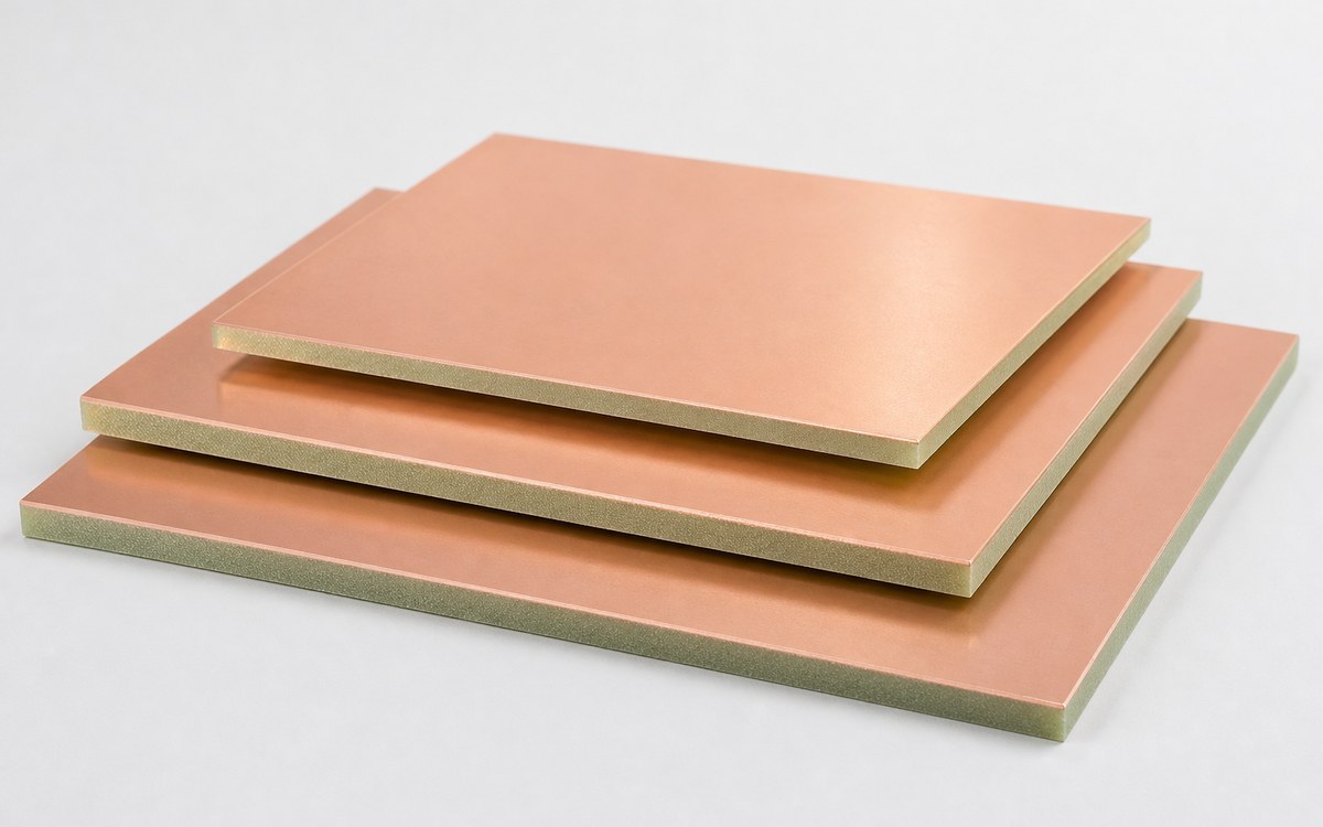
Discuss This Material Requirement
Raw FR-4 and high-Tg copper-clad laminate sheets
Copper-clad laminate used in PCB fabrication.
02High-Speed & RF MaterialsLow-loss laminate routes for signal integrity, controlled impedance and radio-frequency designs.

High-speed and RF designs require the laminate, copper profile and stack-up to be considered as one electrical system. Low-loss hydrocarbon-ceramic, PTFE-type and high-speed digital material families can be reviewed before the construction is released.

Material options

Low-loss high-speed laminates, hydrocarbon-ceramic systems and PTFE-type materials.

Suitable constructions

Controlled-impedance multilayer, RF, antenna and mixed RF-digital stack-ups.

Typical applications

Telecommunications, sensing, RF modules, high-speed computing and test equipment.

Confirm before quote

Frequency, Dk/Df method, copper profile, impedance, thickness tolerance and specified material number.
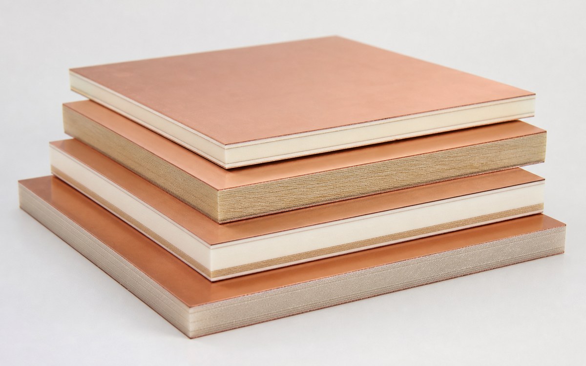
Discuss This Material Requirement
Raw high-speed and RF copper-clad laminate materials
Low-loss laminate blanks before imaging, drilling and circuit formation.
03Polyimide Flexible MaterialsFlexible copper-clad laminates, coverlays and supporting materials for compact interconnects.

Flexible and rigid-flex constructions depend on the bend condition, copper type, adhesive system, coverlay and local reinforcement. The material route is reviewed with the mechanical context rather than selected from thickness alone.

Material options

Adhesiveless or adhesive flex laminate, polyimide coverlay and stiffener materials.

Suitable constructions

Single- and double-sided flex, multilayer flex and rigid-flex integration after review.

Typical applications

Compact interconnects, sensors, movable assemblies and space-constrained electronics.

Confirm before quote

Static or dynamic bend, bend radius, copper type, layer build, coverlay openings and stiffeners.
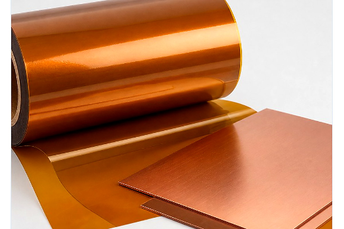
Discuss This Material Requirement
Raw polyimide film and flexible copper-clad laminate materials
Polyimide and copper-clad materials used in flexible PCB fabrication.
04Aluminum & Copper Core MaterialsMetal-backed substrate routes that connect component heat to a controlled thermal path.

Metal-core construction is selected around the thermal path, dielectric system, copper requirement and downstream assembly profile. Aluminum and copper base options can be assessed with the operating power and mechanical interface.

Material options

Aluminum-core and copper-core substrates with project-specific dielectric systems.

Suitable constructions

Single-layer, double-layer and selected multilayer metal-backed PCB structures.

Typical applications

LED lighting, power conversion, motor control, charging and thermal management assemblies.

Confirm before quote

Power map, thermal target, base metal, dielectric, copper, isolation and mechanical interface.
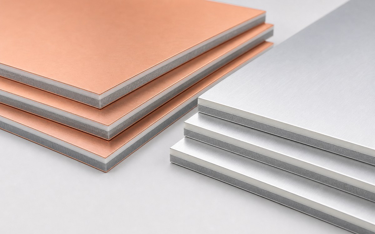
Discuss This Material Requirement
Raw aluminum-core and copper-core PCB substrate sheets
Metal-core substrate materials showing the base and dielectric layers.
05Ceramic SubstratesAlumina and aluminum nitride routes for electrical insulation, dimensional stability and heat transfer.

Ceramic substrates support demanding thermal and insulation requirements, but the correct route depends on material type, metallization, geometry and assembly conditions. Alumina, aluminum nitride and applicable DBC or DPC process routes are confirmed after file review.

Material options

Alumina and aluminum nitride substrate families with reviewed metallization routes.

Suitable constructions

Ceramic circuit substrates using an appropriate thick-film, thin-film, DBC or DPC route.

Typical applications

Power modules, LED systems, sensors, precision electronics and high-temperature assemblies.

Confirm before quote

Ceramic type, thickness, metallization, thermal target, isolation, geometry and assembly profile.
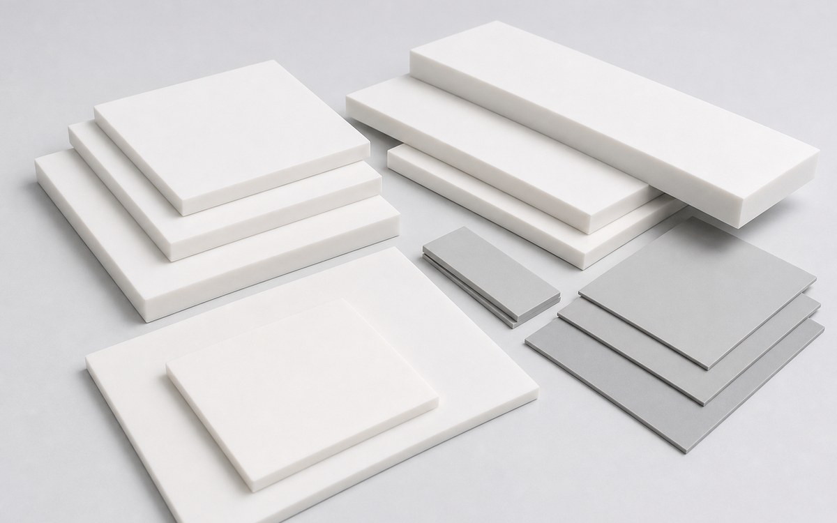
Discuss This Material Requirement
Raw alumina and aluminum nitride ceramic substrate blanks
Ceramic substrate blanks in multiple sizes and thicknesses.
06Specialty & Hybrid ConstructionsMixed-material stack-ups for projects where one laminate family does not meet every requirement.

Some boards need a combination of electrical performance, thermal control, mechanical stability and cost management. Hybrid stack-ups can combine compatible laminate, prepreg, resin-coated copper and copper-foil options after bonding and process risks are reviewed.

Material options

Low-loss and FR-4 combinations, resin-coated copper, selected prepregs and copper foils.

Suitable constructions

Hybrid high-speed stack-ups and other mixed-material builds confirmed by engineering review.

Typical applications

Complex communications, power, aerospace-supporting and specialized industrial electronics.

Confirm before quote

Material compatibility, bonding cycle, CTE, copper balance, reliability evidence and approved substitutions.
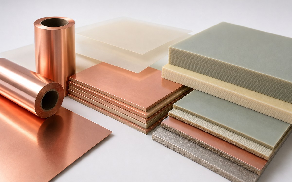
Discuss This Material Requirement
Raw copper foil prepreg and specialty PCB laminate materials
Raw materials prepared for hybrid PCB construction review.
Documented engineering evidenceNeed to see how manufacturing files are screened?

Review an anonymized DFM sample with recorded checks and identified exceptions.

View Anonymized DFM Sample
Commercial route

Know the Review and Quotation Mechanism Before Sending Files

01

Submit available files

Send Gerber or ODB++, drill, drawing, stack-up target, quantity and delivery destination.

02

First response within 12 hours

We confirm receipt, file availability, missing inputs and whether an NDA or controlled transfer route is needed.

03

Engineering review

Capability fit, manufacturing risks, open questions and required outputs are checked before quotation.

04

Quotation and revision control

Schedule and process route are confirmed after review. Revised files are identified and reassessed before release.

Engineering responsibility

A Project Engineer Connects Design Questions to Factory Release

Project engineering team reviewing PCB layout before factory release

Engineering Before Production

The production process is clarified before the board enters fabrication, so customer questions remain tied to the manufacturing data being released.

  • CAM and DFM review
  • Stack-up, copper and impedance confirmation
  • Panelization and process-route questions
  • Revision identification and production-file confirmation
  • PCB-to-PCBA handoff when assembly is included

Choose the Right Route for Your PCB Files

Start with the information you can share. For confidential data or packages that should not travel as ordinary email attachments, request the controlled transfer method before sending files.

Confidential or large files

Request the transfer route and NDA handling first. EBest PCBA will confirm the available method in the first response.

Request transfer route
Available review package

Email the files you are comfortable sharing now, together with quantity, delivery destination and open questions.

Email project package

Send PCB fabrication inquiries to sales@ebestpcba.com. Our engineering team reviews the files and confirms missing information before quotation.

Quote checklist

  • Gerber or ODB++ and drill files
  • Board drawing and stack-up target
  • Material, copper, finish and impedance requirements
  • Prototype and production quantities
  • Target delivery date and destination
  • BOM and assembly files when PCBA is required
FAQ

PCB Fabrication Questions Before an RFQ

Do you fabricate the boards yourselves?
Yes. EBest PCBA manufactures through group-owned PCB facilities for FR4, FPC, rigid-flex, MCPCB, ceramic and specialty builds. The project-specific factory route is confirmed during quotation.
What files should I send for an accurate review?
Send Gerber or ODB++, drill files, board drawing, stack-up target, impedance notes, surface-finish preference, quantity, delivery destination and BOM when assembly is also required.
Can I request an NDA before sending PCB files?
Yes. Use the NDA request link and state whether you prefer EBest PCBA's mutual NDA or want us to review your template before file transfer.
How quickly will EBest PCBA respond?
The published first-response target is within 12 hours. A confirmed quotation schedule depends on file completeness, board complexity, materials and open engineering questions.
How are file revisions controlled?
The approved inputs form the quotation and manufacturing baseline. Revised files should carry a clear revision identifier and are reassessed before production release.
Can PCB fabrication and PCBA be quoted together?
Yes. Send the BOM, centroid data and assembly notes with the PCB package when you want fabrication, sourcing and assembly reviewed as one project.