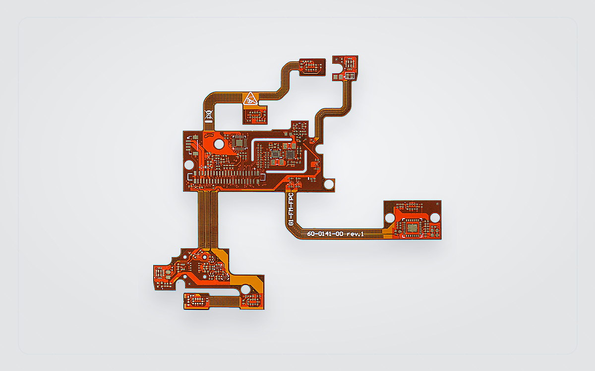
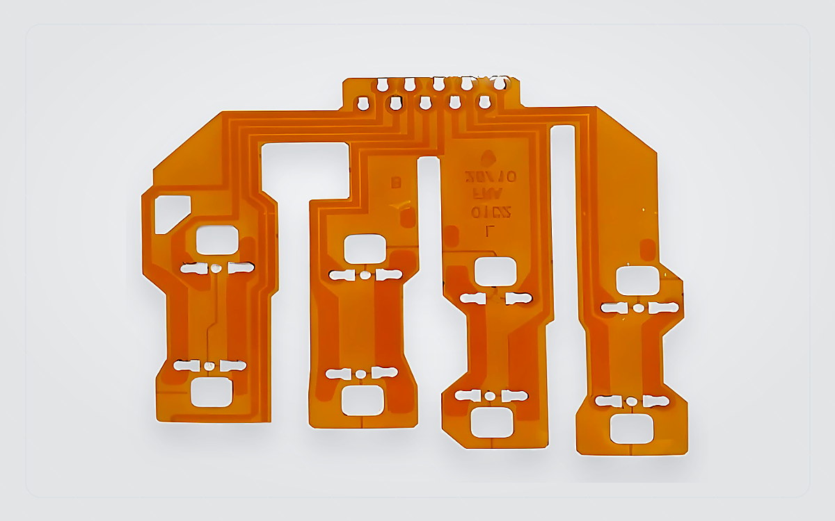
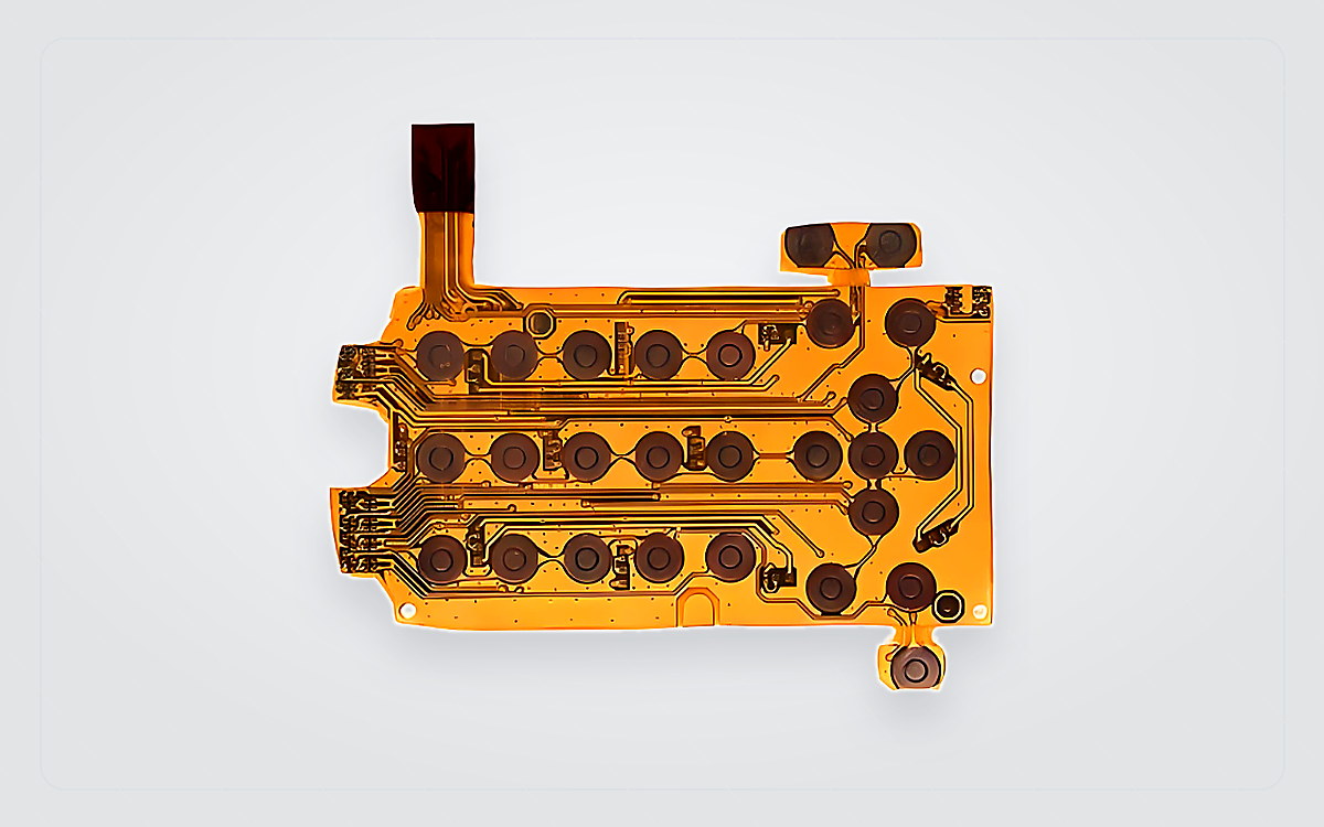
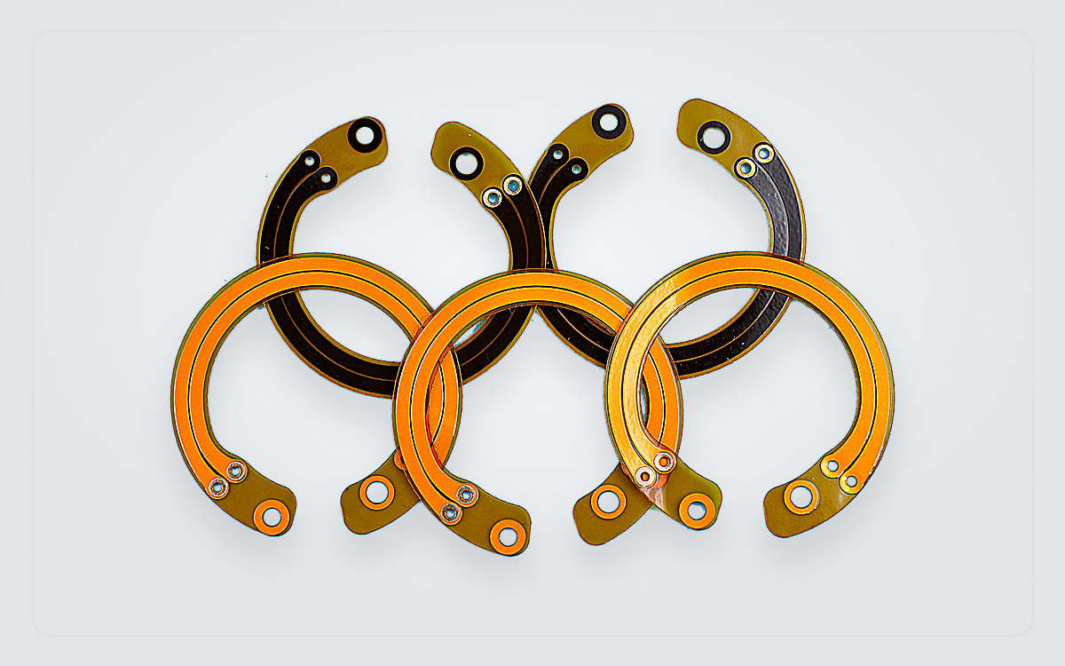
Single-Sided FPC
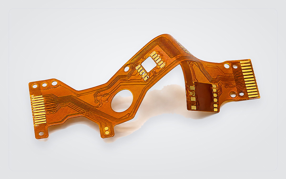
One conductive layer for compact, lightweight interconnects with simple routing and controlled connector areas.
- Review
- Bend zone, coverlay opening, stiffener and contact finish
- Fit
- Simple static or movement-sensitive interconnects
Send your files and tell us where the circuit bends. We will check the materials, copper, coverlay, stiffeners, bend areas, and electrical test needs before quoting.
We aim to reply within 12 hours. Lead time and testing are confirmed after we check your files.
Use this table for a first check. Your stack-up, materials, bend conditions, finish, panel, and test needs determine what we can build.
| Capability item | Routine production reference | Engineering / project-specific review |
|---|---|---|
| Layer count | 1–4 layers | 5–6 layers; higher legacy constructions require route validation |
| Finished thickness | 0.06–0.60 mm | 0.05 mm legacy reference; construction and handling review required |
| Line / space | 3 / 3 mil | 2 / 2 mil with selected thin-copper construction and process review |
| Copper options | 0.33 oz, 0.5 oz and 1 oz commonly assessed | 2 oz on selected structures; bend and etching effects reviewed |
| Base construction | Adhesive and adhesiveless polyimide systems | Final material family selected against thickness, bend and temperature needs |
| Impedance | Target reviewed with stack-up and geometry | ±10% screening reference; coupon and acceptance method confirmed by project |
| Surface finish | ENIG, plated gold, OSP and tin routes | ENEPIG and connector-specific plating require feature review |
The earlier 7–10 layer and 0.05 mm figures were for special or older builds. They are not standard limits. Ask us to check your materials and stack-up.
Choose the FPC structure from the available space, conductor access, bend requirements, connector locations and assembly method.

One conductive layer for compact, lightweight interconnects with simple routing and controlled connector areas.

Conductors on both sides with plated interconnection where routing density exceeds a single-layer solution.

Exposes selected conductor areas from both sides without using a full double-sided circuit.

Multiple conductive layers for higher routing density, with localized flexibility and careful control of the bend stack.

A material name is not enough. We need the full stack-up and bend conditions before we can confirm the build.
Adhesive and adhesiveless systems selected against finished thickness and dimensional behavior.
Choose the copper type and grain direction for either static or repeated bending.
Check coverlay alignment, adhesive flow, and exposed pads before production.
PI, FR4, steel, aluminum and PSA choices tied to connector and installation interfaces.
Installation radius, fold direction and retention are checked for formed-in-place circuits.
For moving parts, provide the bend direction, cycle target, operating conditions, and mechanical support.
We check the drawing against the bend, connector, and assembly needs, then flag any issues before production.
Checks trace direction, abrupt width changes, corners and feature placement through the flexible region.
Reviews support edges, overlap, adhesive and stress transfer around contacts or mounted components.
Confirms pad exposure, registration allowance and coverlay interaction with fine traces and connector areas.
Keep vias and plated holes out of repeated bend areas. Add support where needed.
Aligns copper, dielectric thickness, trace geometry and reference structure with the target impedance.
Accounts for tooling, carrier support, assembly handling and the final separation method.
The process varies by design. Materials, imaging, coverlay, finish, and testing must all follow the approved files.
Confirm structure, bend zones, tolerances and open questions.
Set the polyimide, copper, adhesive, coverlay, and stiffener materials.
Form conductors against the approved geometry and copper choice.
Control openings, registration, bonding and flexible zones.
Complete contacts, plating, stiffeners and final outline.
Apply dimensional, visual and electrical checks to the agreed plan.
These examples show the details we need to quote each type of FPC.

For repeated movement, the bend direction and cycle life affect the copper, trace direction, and bend-area stack.

A space-constrained route where layer build, local flex zones, registration and electrical performance must be balanced.

For connector areas, the plating, thickness, stiffener, and transition shape affect reliability.
Material, cleanliness, testing, and traceability needs depend on the product and where it will be used.

Compact instrumentation and internal interconnects where documentation and controlled assembly matter.

Space-sensitive modules and interfaces requiring clear environmental and validation requirements.

Moving axes, sensors and compact instrument assemblies where bend definition is essential.

Lightweight imaging, control and sensing systems with tight installation envelopes.
You can start with partial files. A complete package helps us quote faster and with fewer follow-up questions.
Send the design files, available space, and movement requirements. We will check the details and reply with the next step.