
High heat density
Move heat from LEDs, power semiconductors or concentrated device areas toward a defined metal and heat-sink interface.
EBest PCBA manufactures aluminum- and copper-base PCBs for lighting and power assemblies. We align the dielectric, circuit copper, mechanical features and heat-sink interface with your thermal and electrical requirements. Direct thermal path constructions are reviewed for selected devices.
We aim to provide an initial response within 12 hours. Materials, construction, inspection scope and production lead time are confirmed from your project files.
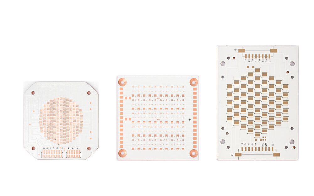
Material references: 1, 1.5, 2 and 3 W/m·K.
Subject to construction and insulation review.
Metal-base thickness is specified separately.
Geometry and copper combination reviewed together.
An MCPCB helps transfer heat away from high-power components and spread it through the metal base. The right construction depends on power density, electrical insulation, current requirements, assembly design, and the cooling method used in the final product.
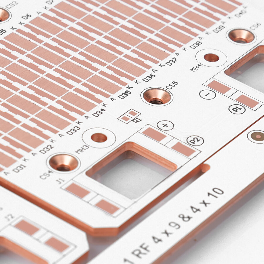
Move heat from LEDs, power semiconductors or concentrated device areas toward a defined metal and heat-sink interface.
Coordinate copper weight and conductor geometry with thermal spreading; thermal conductivity alone does not determine board performance.
Review flatness, finished thickness, holes, outline, V-cut and contact surface against the enclosure or heat sink.
Confirm the soldering profile, component keep-outs, fixture support and back-side contact before assembly.
Aluminum and copper are metal-base choices. Direct thermal path is a device-specific construction feature; pad electrical potential, base contact and surrounding circuit isolation must be defined.
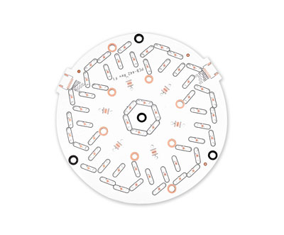
A common option for heat spreading with lower weight and cost considerations. The dielectric, circuit copper, thickness and mounting interface are selected for the application.
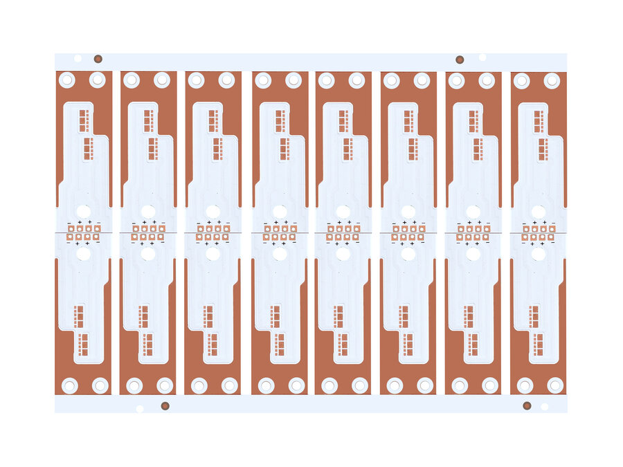
Selected when heat concentration and the mechanical interface justify the added weight and cost. Electrical current capacity follows the circuit copper and geometry, not the base material alone.
Select the metal base, dielectric and circuit construction together. Final geometry and thermal performance depend on the approved stack and system interface.
| Capability | Production Reference |
|---|---|
| Metal base | Aluminum and copper; stainless steel on selected constructions |
| Thermal dielectric conductivity | 1, 1.5, 2 and 3 W/m·K — thermal dielectric material reference values. |
| Circuit layers and construction | 1–10 layers on supported constructions |
| Finished thickness | 0.6–4.0 mm |
| Metal-base thickness — excluding copper | 0.30, 0.40, 0.50, 0.60, 0.80, 1.0, 1.2, 1.6, 2.0, 2.4 and 3.0 mm |
| Circuit copper | 0.5–10 oz, subject to construction review. Minimum line width and spacing depend on copper thickness. |
| Maximum board size | 610 × 1625 mm reference; confirmed for the material, construction and finished-board or panel requirements. |
| Line width / spacing | 4 / 4 mil reference |
| PTH / NPTH diameter tolerance | PTH: ±3 mil; NPTH: ±2 mil |
| Hole position tolerance | ±3 mil reference |
| PTH wall copper | 15 μm reference for standard constructions |
| Through-hole aspect ratio | 10:1 maximum reference |
| Solder mask | White, black, green, blue, yellow and red |
| Minimum solder-mask bridge | 8 mil reference |
| CNC outline tolerance | ±6 mil reference (approximately ±0.15 mm) |
| Surface finish | ENIG, ENEPIG, OSP and lead-free HASL |
| Direct thermal path | Selected device-pad constructions by review |
Dielectric conductivity is a material reference, not a guarantee of operating temperature. The quote confirms the construction, geometry, circuit-to-metal isolation and agreed tests.
A metal-core stack combines the aluminum or copper base, thermal dielectric, circuit copper, surface finish and back-side interface. These elements must meet the thermal, electrical, mechanical and assembly requirements together.
Common for lighting and power products that need a balance of heat spreading, mechanical rigidity, cost and production efficiency.
Selected for heat spreading and mechanical needs where the added weight and cost are justified. Circuit current capacity depends on the conductors and their geometry.
Conductivity, dielectric thickness, voltage withstand, adhesion and thermal cycling are confirmed together rather than maximizing one value.
Copper weight, solderable finish, optional back-side protection, flatness and interface material complete the board’s thermal and assembly interface.
Device attachment, copper area, dielectric thickness, metal base and the heat-sink interface all affect operating temperature. We review the board stack and mechanical contact against your thermal targets.
We check the material stack, conductor geometry, holes, metal clearances, outline and heat-sink contact. The review separates circuit-to-metal isolation, mounting features and any approved direct thermal path.
Confirms metal base, dielectric, copper, solder mask, finish and any direct-thermal-path feature.
Checks conductivity and dielectric thickness against electrical isolation and operating environment.
Reviews copper weight, line width, spacing, pads and local heat-spreading areas together with etching limits.
Coordinates PTH, NPTH, slots, edge distance, plated features and insulation around the metal base.
Examines tolerances, V-cut, routing, chamfer, flatness, fasteners and the heat-sink contact surface.
Checks surface finish, soldering profile, fixture support, component height and back-side contact.
The process covers material preparation, circuit formation, drilling and insulation, solder mask and surface finish, profiling, electrical testing and final inspection. Exact steps depend on the approved construction.
Confirm Gerber files and drawings, aluminum or copper selection, layer structure, thermal requirements, voltage withstand and assembly inputs.
Verify material family, conductivity class, dielectric thickness, metal base, finished thickness and copper weight.
Control imaging and etching according to the specified copper weight and line geometry.
Process PTH, NPTH, slots and special separation features against hole, plating and insulation requirements.
Apply solder mask, legend and the specified HASL, OSP, ENIG, silver, tin or plated-gold finish.
Control routing, outline tolerance, slots, edge clearance, V-cut angle and residual thickness.
Complete continuity testing, agreed isolation checks and final dimensional and visual inspection. Test voltage, duration, locations and acceptance criteria are defined by the order.
Special materials, finer geometry, heavier copper, unusual thicknesses and thermoelectric-separation structures require additional review before production.
The configurations below illustrate construction options. Circuit layers, metal position, interconnections and isolation are confirmed from the approved cross-section.
One circuit layer over a thermal dielectric and aluminum base.
Selected two-circuit-layer stacks with the approved metal and dielectric arrangement.
Circuits on both sides of an approved metal-core construction, with defined interconnection and isolation.
Selected multilayer circuits integrated with a metal base and approved insulating structure.
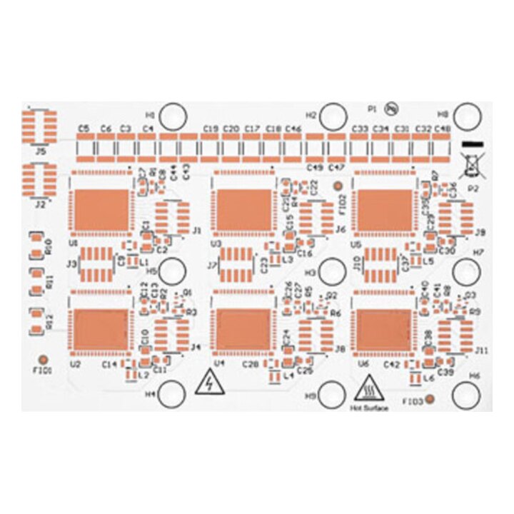
A copper base selected for heat spreading and mechanical needs. Circuit copper and geometry determine current capacity.
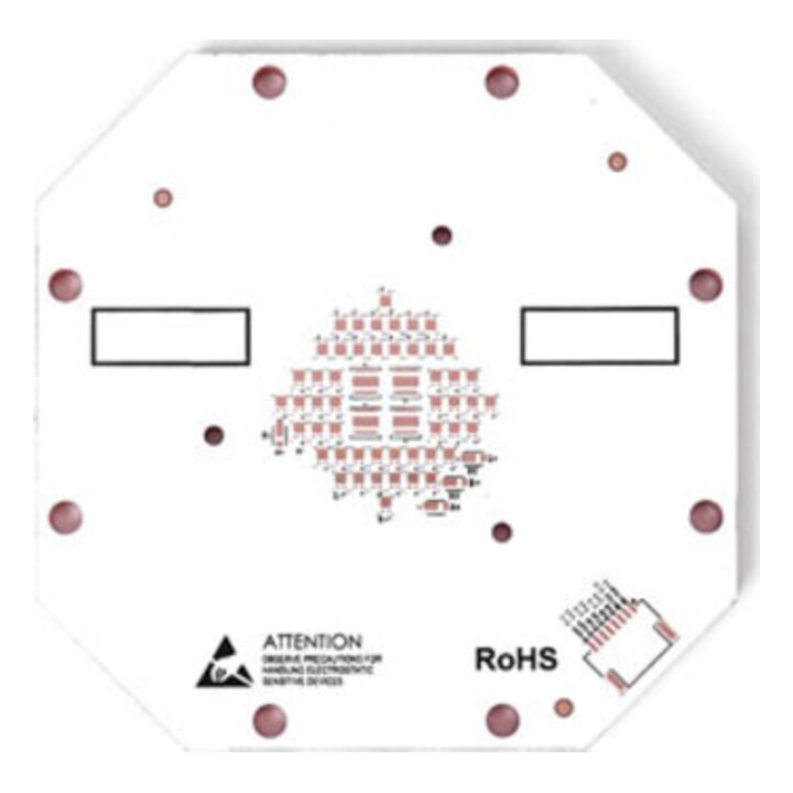
A device-specific thermal-pad connection to the metal base with defined pad potential and surrounding circuit isolation.
Metal core PCBs are commonly used where heat dissipation, electrical isolation and mechanical mounting must be managed together.
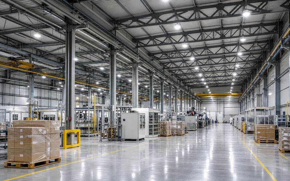
High-bay, roadway and industrial lighting where LED junction heat, dielectric isolation and heat-sink contact drive the board construction.
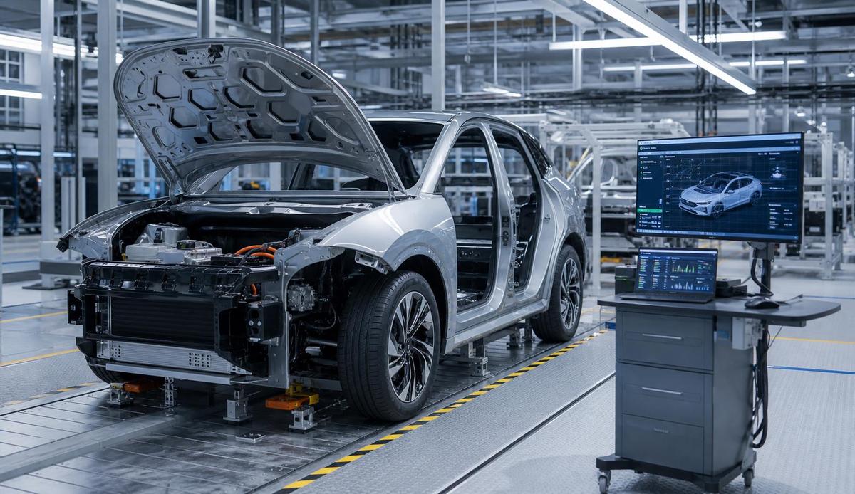
Lighting, power conversion and control products requiring thermal cycling, traceability and controlled mechanical interfaces.
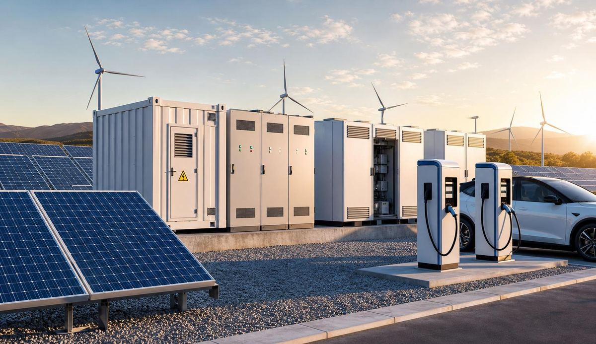
Inverters, charging equipment and power assemblies where heat spreading, current and enclosure contact must be coordinated.
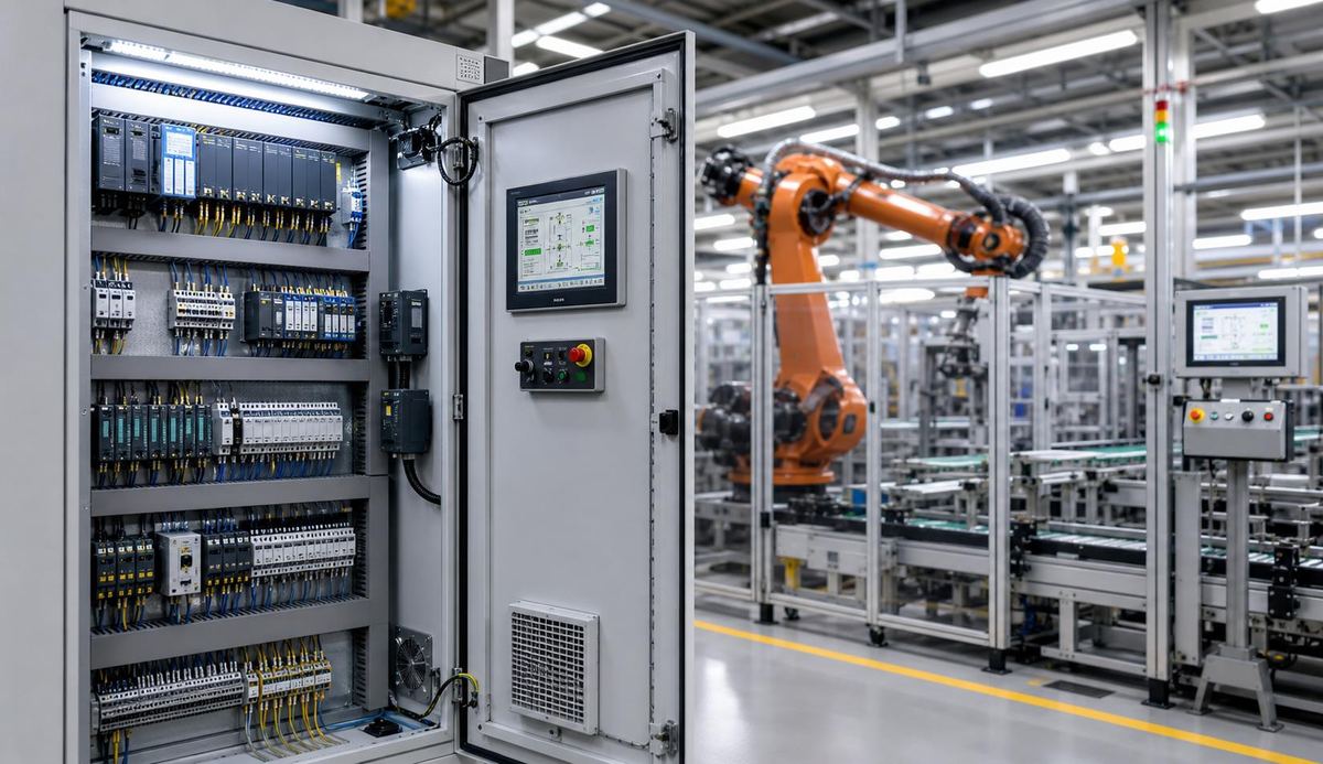
Drives, power modules and control electronics designed for stable operation inside demanding equipment environments.
Start with your board files, drawing and quantity. Add the thermal, electrical and mounting requirements you know; we will identify the information needed to finalize the construction and quote.
Share your design and thermal or mounting requirements. We will review the metal-base construction and confirm open questions, pricing and production lead time.