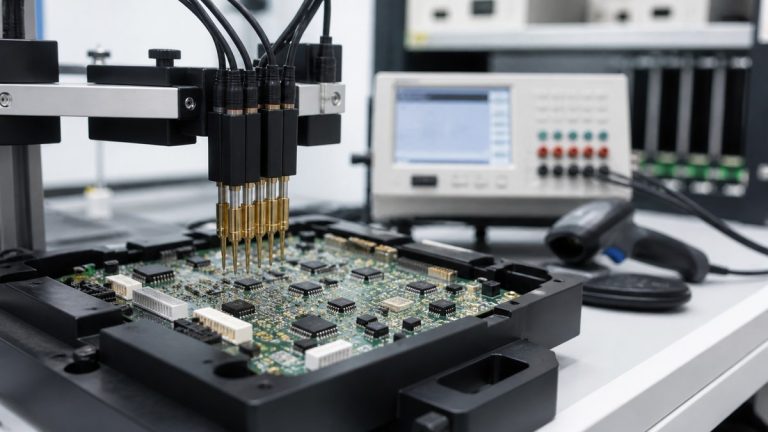
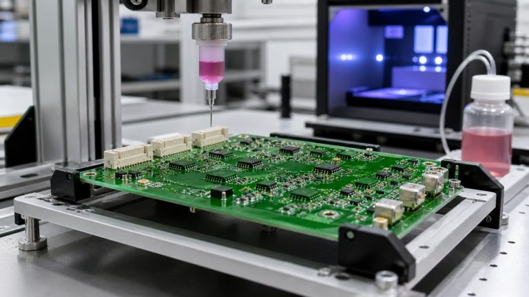
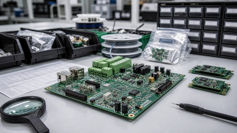
We manufacture motor-drive PCBs and PCBAs with controlled copper, stack-up, thermal-via, exposed-pad, soldering and mechanical-interface requirements. Our engineers review how the design moves heat through the board and how those features affect fabrication, assembly and inspection.
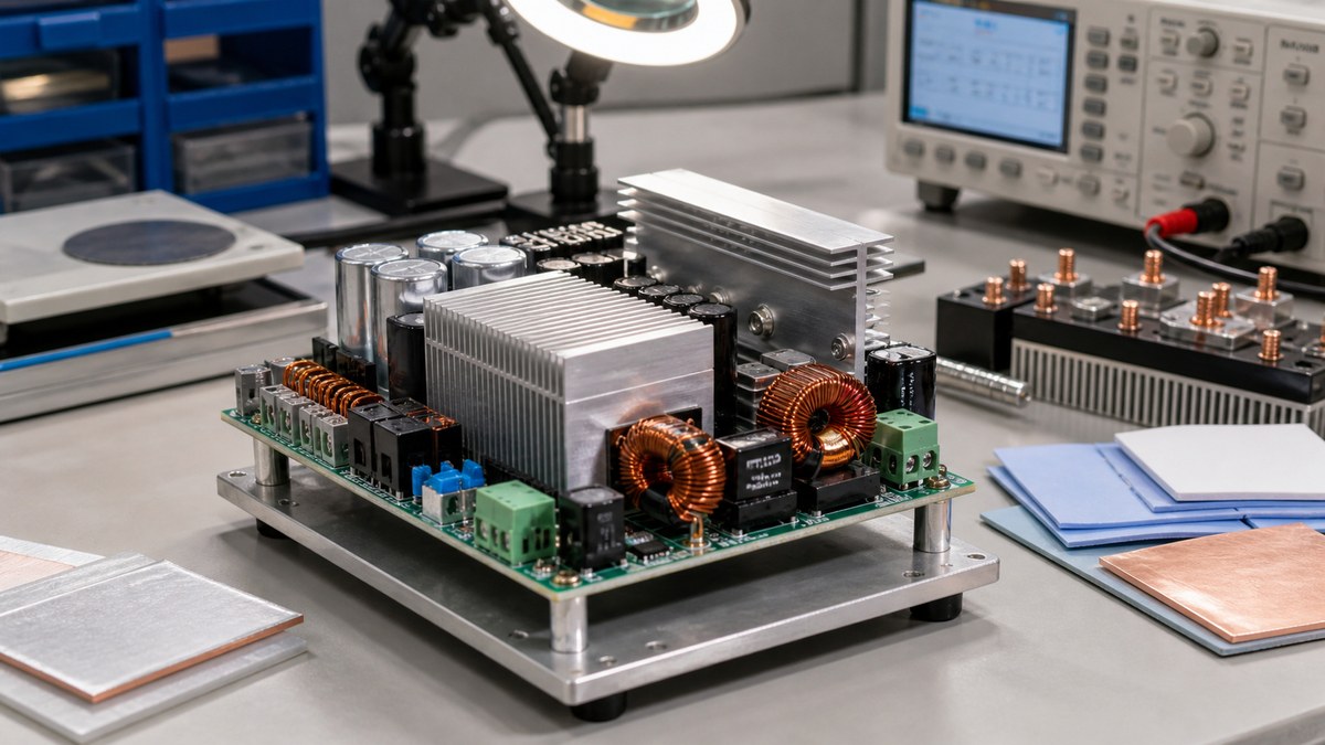
You receive manufacturing questions and a control route tied to the approved design. We preserve the customer’s electrical and system thermal intent while showing how the specified features will be built and what evidence can verify them.
Thermal Feature Control Matrix
| Feature | Our manufacturing review | Evidence |
|---|---|---|
| Heavy or distributed copper | Layer, starting and finished copper, spacing and balance | Approved stack-up and construction |
| Thermal-via array | Diameter, pitch, finish, fill or cap and paste interaction | Drill data and applicable inspection |
| Exposed power pad | Land, mask, paste segmentation and hidden-joint coverage | Stencil decision and applicable SPI/X-ray result |
| Heat sink or interface | Flatness, holes, hardware, material and assembly sequence | Controlled mechanical instruction |
| High-current connector | Copper, hole, soldering, support and inspection access | Process and joint-inspection evidence |
We Need the Thermal Intent Behind the Files
We ask for current, loss, hot components, expected board temperature, heat-sink or enclosure interface, airflow, duty cycle and qualification conditions. These inputs explain why the copper, via and mechanical features matter.
Your team owns operating-temperature and system validation. We use the requirement to review whether the released thermal path can be manufactured without changing geometry or materials silently.
Copper Requirements Must Agree Across the Package
We compare the stack-up, drawing and image data for base copper, finished copper, plated regions and layer-specific requirements. “Heavy copper” without layer and finished-thickness definition is not enough for release.
We also review minimum trace and spacing, copper balance, board thickness and resin fill. You receive a buildable construction or the engineering questions needed to approve one.
We Review Thermal-Via Arrays as Production Features
Our review covers finished hole size, pitch, annular ring, via-in-pad condition, filling or capping, solder-mask definition and the relationship to stencil openings. Open vias beneath an exposed pad can pull solder away from the joint if the design and process are not aligned.
The approved via treatment remains in the fabrication and assembly baseline, with applicable structural or X-ray evidence defined for the project.
Exposed Pads Require Paste and Inspection Decisions
We review pad dimensions, solder-mask opening, paste segmentation, package guidance and thermal mass. The stencil design should support solder coverage while controlling floating, voiding and paste loss.
Where hidden-joint risk justifies it, SPI and X-ray provide different evidence before and after reflow. We define the required coverage and acceptance basis rather than relying on visual inspection alone.
Thermal Mass Changes the Soldering Route
Large copper areas, power terminals, heat sinks and mixed-technology assemblies absorb heat differently. We review reflow or selective/manual soldering needs, fixture support, component temperature limits and access for inspection.
A process that works on a light prototype board may not reproduce on the released heavy-copper construction. The intended production build is used to establish the route.
Heat Sinks and Interfaces Need Mechanical Control
We check mounting holes, flatness, hardware, torque requirement, interface material, keep-outs and assembly sequence where these inputs are provided. Mechanical pressure can affect the board and solder joints as well as thermal contact.
Approved materials and instructions identify what production must install and how the interface will be inspected. System-level thermal performance remains verified under the customer’s representative conditions.
Our Inspection Proves Manufacturing Conditions
We use applicable AOI, X-ray, dimensional or structural inspection to verify build conditions. These methods can show placement, solder, via or mechanical conditions defined in the plan.
They do not replace temperature measurement under operating load. We clearly separate manufacturing evidence from system thermal qualification so your team knows what each result proves.
Why Motor-Drive Customers Use Our Review
We connect thermal design features to buildable copper, drill, stencil, soldering and mechanical controls. Your team can see where heat-path intent could be changed by production and how we prevent that drift.
This reduces late tooling changes, solder defects and unclear responsibility between PCB manufacture, PCBA assembly and system validation.
Send Your Motor-Drive PCB for Thermal Review
Send product files, stack-up, copper definitions, BOM, CPL, assembly drawing, current and duty conditions, thermal-via detail, heat-sink data, interface material, soldering requirements, inspection needs and quantities to sales@ebestpcba.com.
We will return the manufacturing risks, proposed controls and evidence route for your motor-drive PCB or PCBA.