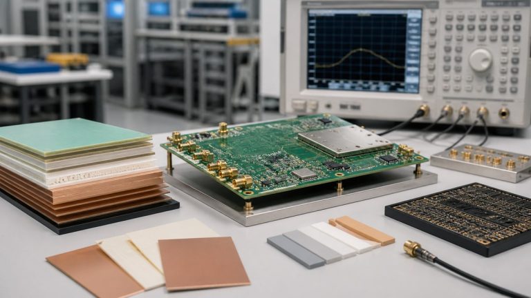
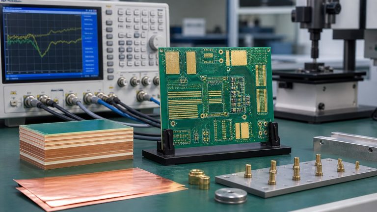
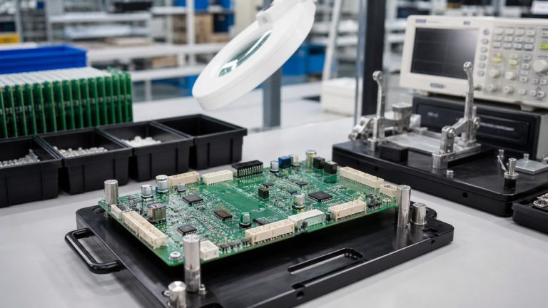
A useful PCB DFM review confirms that fabrication, assembly, sourcing, inspection and test data describe one buildable product. Before we release a project, our engineers compare the complete package with the proposed manufacturing route and return specific questions for approval.
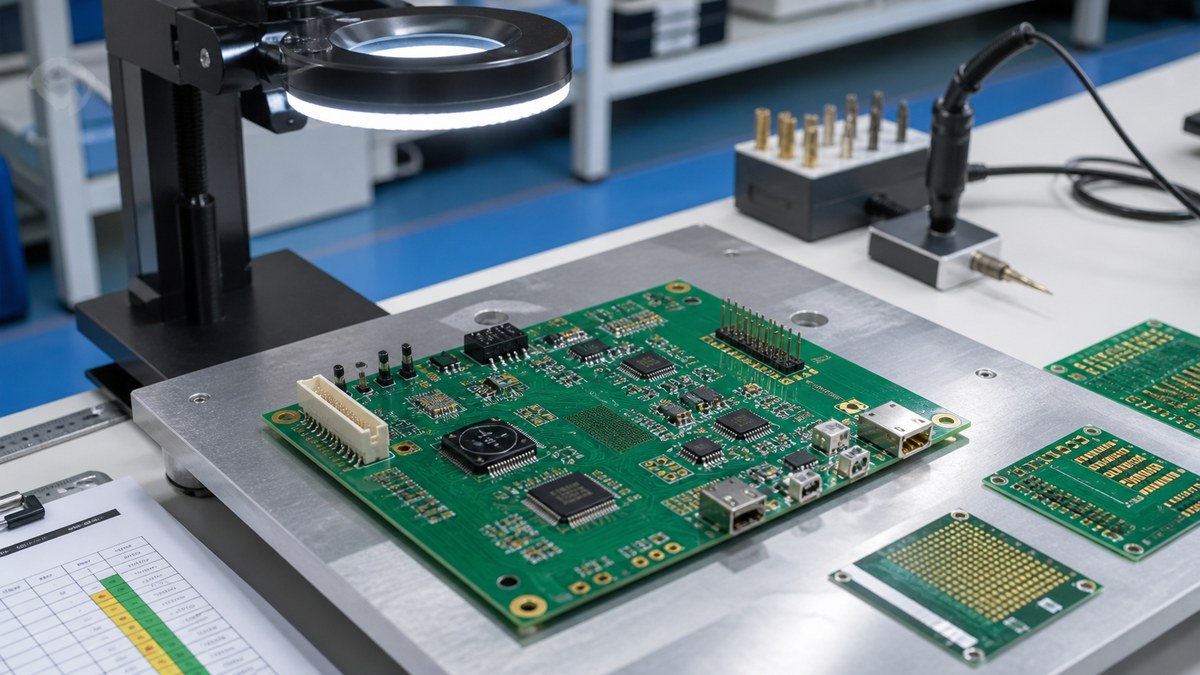
Use the checklist below before requesting a quotation. Complete inputs reduce pricing assumptions, engineering delays, tooling changes and production deviations.
PCB and PCBA DFM Checklist
| Area | Confirm before build | What we return |
|---|---|---|
| Revision | All files use the same part number and revision | Conflict and missing-file list |
| Fabrication | Stack-up, material, copper, drill, finish and tolerances are defined | Approved construction questions |
| Assembly | BOM, CPL, polarity, land patterns and drawings agree | Assembly-risk response |
| Mechanics | Outline, holes, height, connectors and keep-outs are controlled | Interface questions |
| Inspection | Critical visible and hidden features have coverage | Proposed inspection route |
| Test | Access, firmware, fixtures, limits and reports are available | Test-input and coverage plan |
Verify That the File Package Describes One Revision
Gerber or ODB++, drill files, stack-up, fabrication drawing, BOM, CPL, assembly drawing and mechanical data must agree. Check board outline, polarity, connector orientation, part quantities and customer revision.
We return exact conflicts before CAM or machine programming. Approved responses remain linked to the work order.
Give Fabrication Requirements Measurable Values
Define material, finished thickness, layer copper, impedance, drill structure, surface finish, solder mask, dimensions and tolerances. Terms such as “standard,” “high quality” or “heavy copper” do not define a construction.
Our engineers propose a buildable stack-up or return the decisions needed before release.
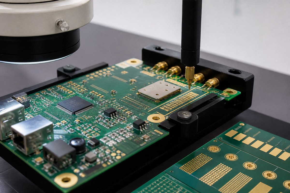
Check Copper, Spacing, Holes and Board Edges
Minimum trace and spacing must fit the layer copper. Drill size, annular ring, aspect ratio, copper-to-hole and copper-to-edge conditions need adequate manufacturing margin.
High-voltage, high-current, RF, flex and controlled-depth features require additional project-specific review.
Make BOM and Placement Data Authoritative
Use full manufacturer part numbers, approved manufacturers and explicit substitution rules. Verify reference designators, quantities, package, polarity and CPL coordinates.
Our BOM and assembly review identifies ambiguous identity, sourcing risk and file mismatch before procurement.
Review Land Patterns, Mask and Paste Together
Fine pitch, QFN, BGA, exposed pads and thermal-via arrays depend on pad, solder-mask and stencil relationships. Excessive paste, open vias or inaccessible joints can create avoidable solder risk.
We connect the package to stencil, soldering and inspection decisions rather than evaluating footprint geometry in isolation.
Panelization Must Support the Product and Process
Board size, shape, edge components, tooling rails, fiducials, breakaway method and depanelization stress affect printing, placement and handling. The best panel depends on both product and quantity.
We propose panel and tooling conditions for customer review where approval is required.
Plan Inspection Before Components Hide the Risk
SPI checks applicable paste conditions, AOI checks visible assembly and X-ray supports selected hidden joints. Define critical dimensions, structural evidence and report requirements before production.
A final functional test cannot replace every upstream inspection.
Plan Test Access Before Tooling
ICT, flying probe, programming and FCT require different test points, fixtures, software and limits. Confirm which functions must be verified and what the report should contain.
We identify access gaps early enough for a deliberate layout or test-strategy decision.
What You Receive From Our DFM Review
- file and revision conflicts;
- fabrication and stack-up questions;
- BOM and sourcing issues;
- assembly and mechanical risks;
- inspection and test coverage proposal;
- approved responses retained with the production package.
Send Your PCB Package for DFM Review
Send Gerber or ODB++, drill files, stack-up, fabrication drawing, BOM, CPL, assembly and mechanical drawings, quantities, special processes, inspection requirements and test package to sales@ebestpcba.com.
Our engineers will return the manufacturability questions and proposed route before production.
What You Receive After Our DFM Review
We return a focused list of conflicts, missing inputs, proposed manufacturing adjustments and approval items. Each comment is tied to the supplied revision so your engineering team can update the source file or authorize a documented exception. Once those points close, we release the approved package to fabrication and assembly and keep the decision record with the project.