We manufacture aerospace RF and controlled-impedance PCBs by connecting the customer’s electrical target to one approved production construction. Our engineers review the stack-up, laminate, copper, dielectric thickness, trace geometry, reference plane, via structure, solder mask and test method before CAM release.
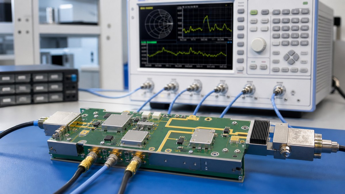
You receive a controlled stack-up proposal, resolved engineering questions and the impedance evidence defined for the build. The calculated structure, fabricated panel, representative coupon and final report remain tied to the same released revision.
What We Control From Target to Test Result
| Required input | Our manufacturing control | Evidence you receive |
|---|---|---|
| Impedance target and tolerance | Identify single-ended or differential structure and reference layer | Approved impedance requirement list |
| Material requirement | Review Dk, Df, test method, frequency and availability | Released material and stack-up |
| Trace geometry | Model production width, spacing, copper and dielectric | Approved geometry response where adjustment is needed |
| Via and backdrill structure | Link drill pairs and remaining stub to final stack-up | Controlled drill information and applicable inspection |
| Impedance verification | Use defined coupon structures and measurement conditions | Lot- and revision-linked impedance report |
We Start With an Unambiguous Electrical Requirement
We ask you to identify the target impedance, tolerance, signal layer, reference plane, single-ended or differential condition, relevant nets or structures and any required test method. Typical industry targets such as 50 ohm single-ended or 90–100 ohm differential are not automatically your product requirement.
If the drawing, stack-up and routing data disagree, we return the conflict before release. This prevents a coupon from being tested against a target that does not represent the intended product structure.
Our Production Stack-Up Defines the Manufactured Result
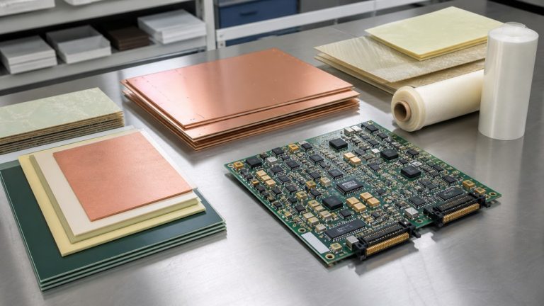
We convert the approved layer function into a buildable combination of cores, prepregs, copper and finished thickness. Resin content, dielectric thickness, copper distribution and fabrication tolerances are reviewed together. The production stack-up becomes the reference for geometry modelling, drilling and coupon design.
When an available material construction requires a change, we show the proposed stack-up and its effect before production. We do not silently replace a dielectric or copper definition that controls the electrical result.
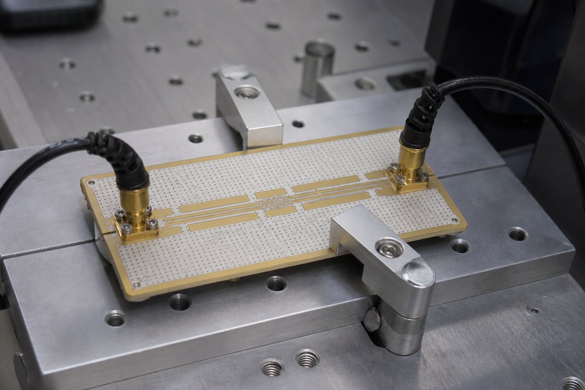
We Review Material Data in the Correct Context
For RF and high-speed designs, dielectric constant and dissipation factor require a frequency and test-method context. Copper foil profile, resin system and actual construction can also influence insertion loss and impedance. A brand name or one datasheet value is not a complete production specification.
Our material review identifies the approved grade, permitted source or equivalent rule and documentation needed for repeat orders. Material changes follow the agreed engineering approval route.
Geometry Adjustments Remain Under Customer Approval
Fabrication compensation may require a proposed change to trace width or differential spacing. Our engineers model the production geometry using the approved stack-up and process basis, then return the proposal through an engineering query when customer approval is required.
We preserve the approved response with the released product definition. This keeps design intent, CAM data and measured evidence aligned instead of allowing an undocumented geometry change on the manufacturing side.
Reference Planes, Launches and Vias Stay Visible
Impedance depends on the return structure as well as the routed trace. We review reference-plane continuity, layer transitions, via fields, connector launches and relevant clearances for manufacturability. Electrical performance remains the customer’s design responsibility, while we identify production details that could change the released structure.
For backdrill or controlled-depth structures, we link drill side, layer pair, diameter, registration, depth basis and remaining-stub requirement to the final stack-up. Applicable inspection evidence is agreed before release.
Our Coupons Represent Defined Production Structures
We place controlled-impedance coupons on the production panel for the structures included in the test plan. The coupon identifies its relevant layer, reference, geometry and target. Panel location and representation are reviewed so the report can be interpreted correctly.
An impedance report proves the measured coupon under the stated conditions; it does not by itself prove complete RF system performance. We keep that boundary clear while giving your team useful fabrication evidence tied to the lot and revision.
We Protect Repeat Orders From Silent Construction Drift
The approved stack-up, material, impedance structures and test basis remain part of the controlled production package. Before a repeat order, we check the released baseline and review any proposed material or process change that could affect the electrical construction.
Available work-order, material and test records support comparison with the approved basis. This helps prevent a repeat build from using a similar-looking but electrically different construction.
Why RF Customers Use Our Controlled Process
We do more than accept an impedance value on a drawing. We connect the value to the material, stack-up, production geometry, coupon and report that can verify fabrication. Your engineers can review every decision that changes the manufactured transmission-line structure.
This gives you a defined path from RF design handoff to repeatable PCB production and clear evidence of what was actually built and measured.
Send Your RF and Impedance Data for Review
Send your Gerber or ODB++ data, stack-up, fabrication drawing, material requirement, finished thickness, copper, impedance table, target tolerance, relevant frequency, via and backdrill details, quantity and report requirements to sales@ebestpcba.com.
We will return the proposed production construction, open engineering questions, required approvals and impedance evidence plan for your aerospace PCB.