
Skip to content
Home / Services / DFM Review

Find the failure on paper,
before the line finds it for you

Send Gerber or ODB++ and BOM files. An EBest PCBA engineer checks your design against real PCB and PCBA process limits, then sends back a practical DFM report within 24 hours. Free. NDA available first. You keep the report either way.
279 checks 12 categories 24h response NDA first
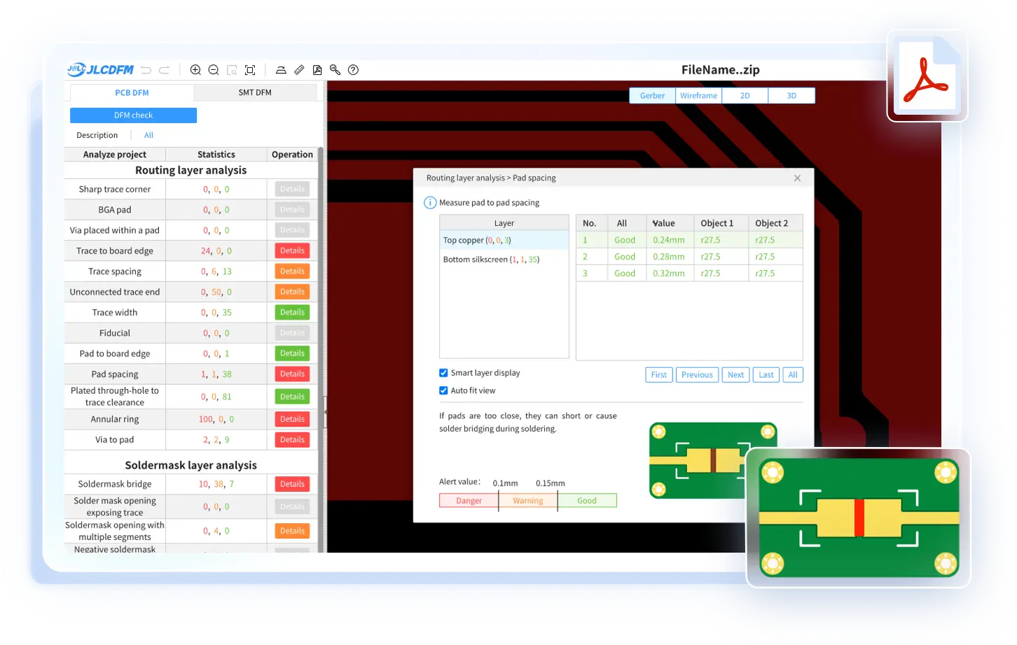
DFM analysis tool showing PCB manufacturability findings
DFM Analysis PreviewVisual findings before fabrication release

A quote tells you price. A DFM review tells you whether the board can be built safely. Before you commit to fabrication or assembly, we check the files against the process limits, footprint realities and assembly risks that CAD DRC often cannot see.

Free DFM before production | Gerber / ODB++ review | BOM health option | Report is yours even if you build elsewhere
Customer risk first

Your CAD DRC Can Pass. Production Can Still Fail.

Most design teams already run DRC before sending files. The problem is that DRC only checks the rules configured in the CAD tool. It may not know the factory's depanel limit, whether a library footprint actually matches the component pin, or whether a package will create solder reliability risk on the line.

Footprint library errorsPins extend beyond pads, pads do not support the package, or repeated library mistakes appear across every build.
Edge and depanel stressParts placed too close to the board outline can crack during routing, V-cut, handling or fixture loading.
Assembly access issuesFiducials, polarity, solder access, BGA inspection and test access can be missing even when layout rules pass.
Who this is for

This Review Is Built For:

If one of these sounds like your project, send the files before release. The goal is to catch manufacturability, BOM and assembly risks while they are still easy to fix.

01

Hardware teams preparing prototype PCBA

Catch footprint, panel and assembly risks before the first build turns into rework.

02

OEMs moving from prototype to pilot run

Turn prototype lessons into repeatable production checks before batch release.

03

Engineers with dense SMT / BGA / QFN boards

Confirm hidden joints, placement limits, X-Ray needs and inspection access early.

04

Buyers comparing PCBA suppliers

Compare engineering feedback and risk prevention, not only unit price.

05

Teams worried about BOM or assembly risk

Pair DFM findings with BOM health, package checks and sourcing-risk feedback.

Not sure if your board needs review?Send what you have. We will tell you what is missing before quoting or production release.
Send Files for Free DFM Review
The findings

The Report Does Not Say "Risk Somewhere." It Names the Part.

A useful engineering report must be specific enough for your layout engineer to fix the file without a meeting. Each flag points to the exact component, side, issue, standard value, actual value and recommended correction.

01

C553 - too close to board edge

A chip was only 2.51 mm from the board outline against a 3.0 mm process limit. That creates depanel and handling stress risk.

Category
Component Layout
Risk
Cracked part or intermittent joint
02

Q42 - pin heel beyond pad

The LFPAK56 MOSFET footprint did not fully support the pin heel. This is a library error that can create poor soldering.

Category
Graphics Library
Actual
-0.08 mm pad coverage
03

R108 - current sense resistor mismatch

The 2512 current-sense resistor footprint showed pin heel beyond pad. On a current-carrying part, this becomes a reliability concern.

Category
Graphics Library
Actual
-0.34 mm pad coverage
04

D25 - pin toe beyond pad

The SOD-123 diode footprint had a pin toe overrun. Small on paper, but it is still a designed-in weak joint.

Category
Graphics Library
Actual
-0.02 mm pad coverage
Real sample report

279 Checks. 3 Findings. Four Parts Named.

This anonymized 12-layer control-board example shows the DFM findings returned before production. Each finding identifies the affected location, manufacturing risk and recommended correction.

279review items checked
276passed items
3rule violations
4 Hotcomponent flags

Board reviewed

  • 12-layer control board: 2.296 mm thickness, 254 x 406 mm size.
  • Assembly density: 304 SMD parts, 41 through-hole parts, four BGAs, 0.5 mm minimum BGA pitch.
  • CAD match: 100% part-number and reference-designator match before the review ran.
PCB-009238
Anonymized report
Why it matters

A Small Finding Can Prevent a Large Production Problem.

The value of DFM is not the 276 items that passed. It is the few items that would otherwise move into fabrication, assembly, test and shipment exactly as drawn.

Before buildFix a footprint, move a part, confirm a process limit.
During buildAvoid line stops, rework loops, poor solder joints and first-article delays.
After shipmentReduce latent field failures caused by weak joints or mechanical stress.
The point: two of the sample issues came from the part library. If nobody checks pin against pad, the same error can repeat across every board and every order.
Engineering proof

CAD DRC Checks Your Rules. EBest PCBA DFM Checks the Factory Reality.

That difference is the reason customers send files before they place an order. We are not trying to replace your CAD workflow. We add the manufacturing reality your CAD rules may not include.

Your CAD DRCEBest PCBA DFM Review
Checks against

Rules configured in your design tool.

Factory process limits, footprint geometry and assembly conditions.

Footprint library errors

Often pass when the library itself is wrong.

Pin-to-pad geometry is reviewed and flagged with evidence.

Process limits

Generic or not configured.

Edge, depanel, soldering, inspection and test-access limits are checked.

Output

Pass/fail rule messages.

RefDes, coordinates, image, MPN, standard vs actual and recommended fix.

What you receive

A Report Your Design Team Can Act On.

Every finding is built to shorten the path from "there is a risk" to "we know exactly what to fix."

Reference designatorExact component, top or bottom side, and linked issue.
XY coordinatesPrecise location so the layout engineer can go straight to the problem.
Captured imageVisual evidence of pad, pin, clearance or assembly geometry.
Standard vs actualThe required process limit and your measured value side by side.
MPN and package dataManufacturer part number, package and footprint detail where relevant.
Recommended fixActionable correction with priority level: Critical, Hot, Warm or Cool.
How it works

From Your Files to a Report in 24 Hours.

The path is intentionally simple. Customers should not need a long sales call before discovering whether a board has manufacturing risk.

01NDA first if needed

We can sign a mutual NDA before you send Gerber, ODB++, BOM or drawings.

02Send what you have

Gerber or ODB++ and a BOM with manufacturer part numbers are enough to start.

03Engineer review

An engineer checks roughly 280 items across PCB, assembly and test-readiness categories.

04Report back

You receive findings, evidence and recommended fixes within 24 hours for typical boards.

05Build quote if wanted

If you want production support, the review becomes the basis for a safer quote and build plan.

Pair DFM with BOM Health.While DFM checks the board, our sourcing team can flag lifecycle, availability, package and approved-alternate risks in your BOM.
Upload Files
Factory-backed review

Engineer-Run, Not Portal-Only.

The review is credible because it is tied to the team that can fabricate, source, assemble, inspect and test the product. Findings do not sit in a generic checklist. They feed directly into a real production plan.

PCB fabrication knowledgeLayer stack, drill, solder mask, outline and panel limits.
PCBA assembly knowledgePaste, placement, reflow, AOI, X-Ray and through-hole constraints.
Component sourcing awarenessMPN clarity, package match, lifecycle risk and approved alternates.
3D and mechanical checksFor complex builds, assembly fit and interference can be checked beyond the bare board.

Send the Files. Keep the Report Either Way.

Upload Gerber or ODB++ and BOM files. We will check the design for manufacturability risks, flag what matters and send back practical findings within 24 hours.

Upload Gerber & BOM for Free DFM Review
FAQ

DFM Review Questions Engineers Ask

Is the DFM review really free?
Yes. The review, report and recommended fixes are free, with no obligation to order. We earn the production order by showing useful engineering work first.
What files do you need?
Gerber or ODB++ and a BOM with manufacturer part numbers are the best starting point. Centroid, assembly drawings and test requirements make the review stronger.
How long does it take?
Typical boards can be reviewed within 24 hours. Very large, dense or incomplete projects may take longer; we will say that before the review proceeds.
How is this different from my CAD DRC?
CAD DRC checks your configured design rules. EBest PCBA DFM checks the files against real fabrication, assembly, inspection and test constraints, including footprint and process-limit risks.
Will you sign an NDA first?
Yes. A mutual NDA can be signed before you send files.
Do I have to manufacture with EBest PCBA to keep the report?
No. The report is yours. If you decide to build with us, the findings become the starting point for a safer quote and production plan.