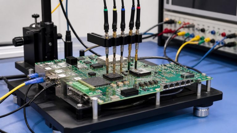
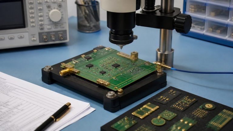
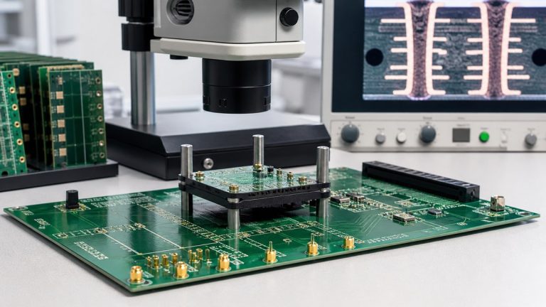
We turn your impedance requirement into a controlled production structure and measurable coupon. Our engineers link the target to a specific signal layer, reference plane, material, dielectric thickness, copper, trace width, differential spacing, solder-mask condition and tolerance.
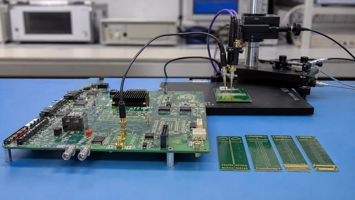
You receive an approved stack-up and, where required, a lot-linked impedance report. The coupon is designed from the released manufacturing construction so the measured evidence represents a defined production feature rather than a generic test trace.
Target-to-Coupon Workflow
| Step | Our action | Output |
|---|---|---|
| 1. Define target | Identify impedance, tolerance, layer, reference and net type | Controlled requirement list |
| 2. Build stack-up | Select approved material and dielectric construction | Production stack-up |
| 3. Model geometry | Calculate production width and spacing | Engineering proposal |
| 4. Create coupon | Represent the approved structures on the panel | Coupon design |
| 5. Measure | Test under the defined method and conditions | Lot- and revision-linked report |
We Require a Complete Impedance Table
The target should identify single-ended or differential condition, nominal value, tolerance, signal layer, reference plane and relevant nets or geometry. Common values such as 50 ohm or 100 ohm are not assumed to apply without a released requirement.
If the drawing, stack-up and image data disagree, we return the conflict before CAM release.
The Stack-Up Becomes the Measurement Basis
We define layer functions, material construction, dielectric thickness, copper and finished thickness using buildable cores and prepregs. Dk must be considered with its frequency and test-method context.
The approved stack-up remains the basis for geometry modelling, coupon creation and repeat orders.
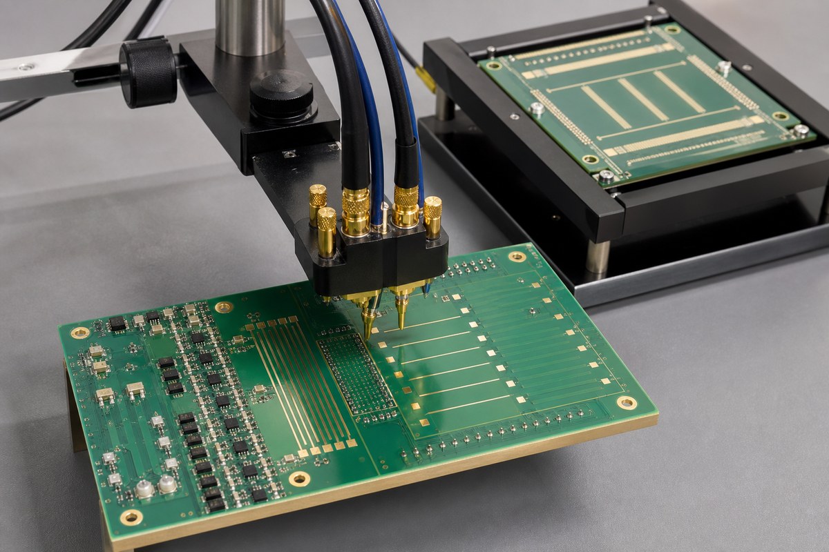
Production Geometry Includes Real Fabrication Conditions
We model trace width, differential spacing, copper thickness, dielectric and solder-mask condition according to the process basis. The nominal CAD geometry may require an approved production adjustment.
We return any geometry change through the engineering-query path and preserve the approved response with the product revision.
We Match Coupons to the Controlled Structures
The coupon identifies the target, layer, reference and representative geometry. Different layer relationships or impedance types may require separate structures.
Panel location and representation are reviewed so the report can be interpreted correctly. A coupon that does not match the released stack-up provides weak evidence.
Measurement Conditions Stay Visible
The report identifies the production lot, product revision, coupon or structure, target, result and applicable method. Where a specific report format or measurement condition is required, it is agreed before production.
The measured coupon shows impedance for that defined structure. It does not prove every routed segment, via transition, connector launch or complete channel.
Out-of-Tolerance Results Follow Controlled Disposition
When a result does not meet the approved requirement, affected product is contained and reviewed. We do not change the target or geometry after measurement to create an apparent pass.
The disposition, additional review, rework possibility or customer decision remains documented and tied to the lot.
Repeat Production Protects the Approved Basis
Before repeat orders, we compare material, stack-up, geometry, coupon and target with the released baseline. Proposed material or process changes are reviewed for impedance effect.
This maintains continuity between the first approved report and later production.
Why Customers Use Our Impedance Process
We provide a transparent path from electrical target to physical construction and measured evidence. Your engineers can review every manufacturing decision that changes the controlled structure.
This reduces ambiguity and makes the impedance report useful for supplier and production control.
Send Your Impedance Requirements
Send Gerber or ODB++, stack-up, material, copper, finished thickness, impedance table, layer references, differential-pair information, tolerance, relevant frequency, panel or coupon requirements, quantity and report format to sales@ebestpcba.com.
We will return the proposed stack-up, geometry questions, coupon plan and evidence route.
What to Send Us for an Impedance Review
Send the target impedance and tolerance, net or layer identification, differential geometry, reference plane, finished thickness, material restrictions and solder-mask condition. We will propose manufacturable geometry and coupon details for your approval. Your approved stack-up then becomes the common reference for CAM, fabrication, measurement and the report supplied with the applicable lot.