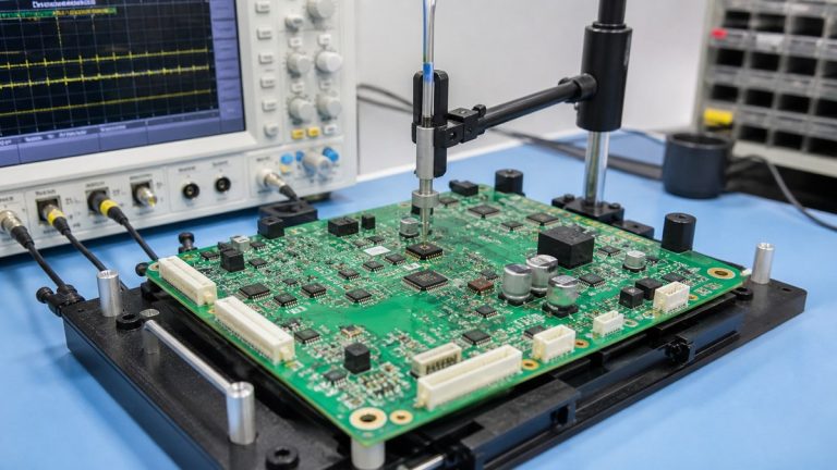
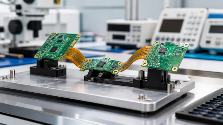
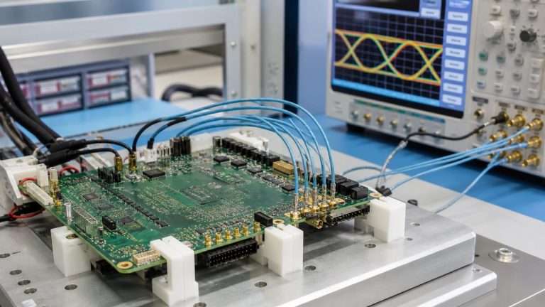
We manufacture motor-drive PCBs by controlling the complete current path: layer copper, traces and planes, plated holes, via arrays, power packages, terminals, solder joints and thermal interfaces. Our engineers compare the electrical intent with the fabrication and assembly process before production release.
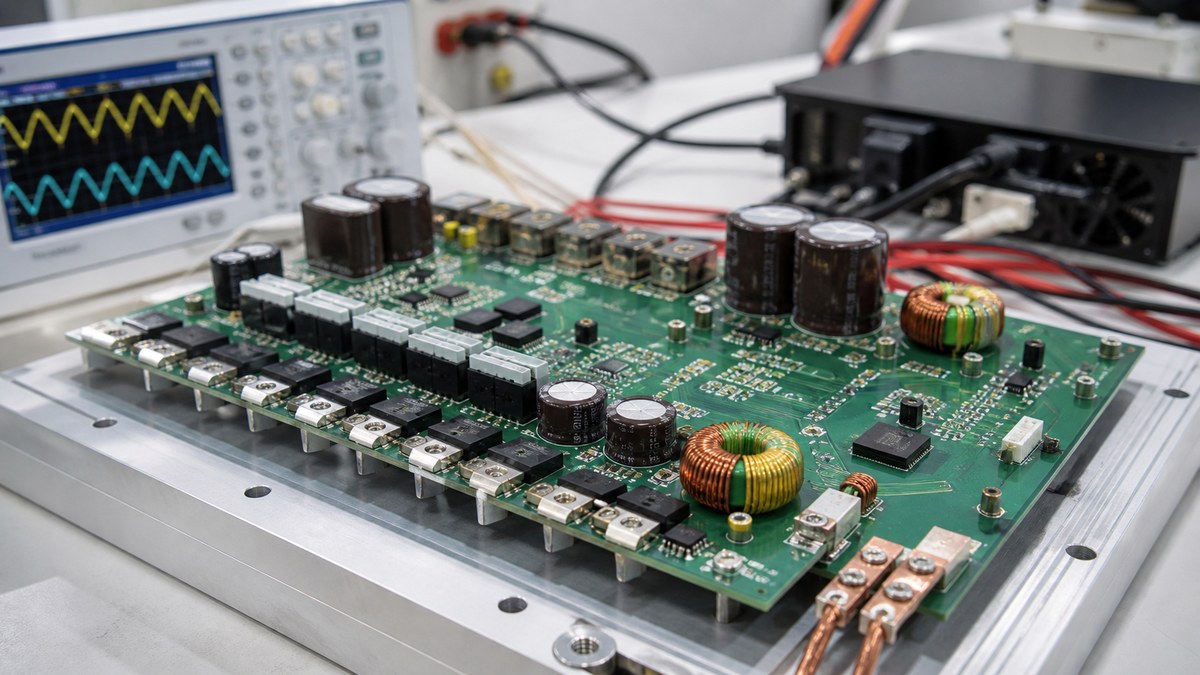
You receive a buildable construction, resolved DFM questions and evidence for the features we can verify. We do not treat thicker copper as the automatic answer; copper, geometry, temperature, voltage, switching behavior and assembly limits must work together.
High-Current Manufacturing Control Map
| Feature | Our review | Evidence |
|---|---|---|
| Copper path | Layer, base and finished copper, width, spacing and balance | Approved stack-up and image basis |
| Plated current transfer | Hole, via quantity, annular ring and plating requirement | Drill data and applicable structural inspection |
| Power package | Land, paste, thermal vias and hidden-joint coverage | Stencil and applicable SPI/X-ray results |
| Terminal or bus connection | Hole fit, soldering, hardware, support and access | Assembly and inspection record |
| Electrical function | Test procedure, load, limit and fixture | Defined test result |
We Need Current, Voltage and Duty Information
We ask for continuous and peak current, duty cycle, voltage, switching conditions, allowable temperature rise, cooling path and qualification requirement. These inputs explain the purpose of the specified copper and connections.
Your engineers own circuit sizing and system validation. We use the requirement to check whether the released physical features can be manufactured and inspected as intended.
Copper Definitions Must Be Complete
We reconcile stack-up, drawing and Gerber data for layer-specific copper. Starting foil, plated contribution and finished copper are not interchangeable descriptions. Minimum trace and spacing must reflect the actual copper requirement.
Heavier copper improves resistance and heat spreading in appropriate designs, but it also affects etching, fine features, resin fill, flatness, cost and assembly thermal mass. We return the trade-offs before the construction is approved.
Vias and Plated Holes Carry Both Current and Process Risk
We review finished hole size, drill size, aspect ratio, annular ring, via quantity, placement, fill or cap requirements and the connection to copper planes. A via array is only useful when its manufactured geometry and plating basis are defined.
Where required, microsection or other structural evidence is planned for representative features. Electrical current capability still requires design and system validation.
Power Packages Need Controlled Paste and Soldering
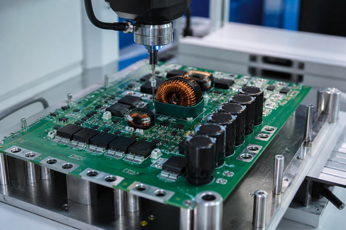
MOSFETs, drivers and other exposed-pad packages combine electrical, thermal and hidden-joint risks. We review pad, mask, paste segmentation, thermal vias and component thermal mass.
SPI can control paste before placement, and X-ray can provide selected evidence after reflow. The approved coverage is tied to package risk and customer criteria.
Terminals and Heavy Parts Need Mechanical Support
We check high-current connectors, terminals, busbars, shunts, inductors and capacitors for hole fit, solder access, insertion force, hardware, support and clearance. Large parts can stress the PCB during assembly and robot operation.
Approved fixtures, fastening or staking requirements become controlled instructions and inspection points.
Voltage Spacing Remains Part of the Review
High current does not remove voltage risk. We compare the released creepage, clearance, slots, coating keep-outs and board-edge geometry with the customer requirement and manufacturing tolerances.
The customer identifies working voltage, environment and applicable safety standard. We ensure the specified physical spacing remains visible and manufacturable.
Testing Must Represent the Defined Function
We review continuity, power-up, programming, current sensing, gate-drive and functional requirements according to the customer procedure. Fixtures, loads, firmware, limits and report format are confirmed before production.
A low-power bench check cannot prove full-load thermal performance. We state what our manufacturing test covers and what remains for system qualification.
Why Motor-Drive Customers Use Our Process
We connect electrical current intent to copper, plating, soldering, mechanical support and verification. Your team can review how each critical feature enters the production route and which evidence supports release.
This reduces late changes and avoids relying on copper weight or a power-on result as the only proof of a high-current assembly.
Send Your Motor-Drive PCB for Review
Send Gerber or ODB++, stack-up, copper definitions, BOM, CPL, assembly drawing, continuous and peak current, voltage, duty cycle, thermal conditions, terminal data, inspection needs and test procedure to sales@ebestpcba.com.
We will return the manufacturing questions, proposed process controls and evidence plan.