
PCB Layout Design
Component placement and routing based on your schematic, BOM, board outline and confirmed design requirements.
Send your schematic, BOM, board outline and design requirements. We will confirm missing inputs, define the layout scope and prepare the agreed fabrication and assembly files for release.

Design support can cover everything from PCB layout and stack-up planning to DFM/DFA review and the final files needed for fabrication and assembly.
Component placement and routing based on your schematic, BOM, board outline and confirmed design requirements.
Layer construction and impedance requirements coordinated with the intended PCB manufacturing process.
PCB fabrication and PCBA assembly risks reviewed before the production files are released.
Agreed design, fabrication and assembly files organized for quotation, prototype and production.
Choose the material platform closest to your product. EBest reviews the schematic, component density, mechanical limits, thermal requirements and manufacturing process before confirming the design schedule.
Typical PCB layout projects take 5–10 working days. Complex structures, special materials and additional review rounds are scheduled after file review.
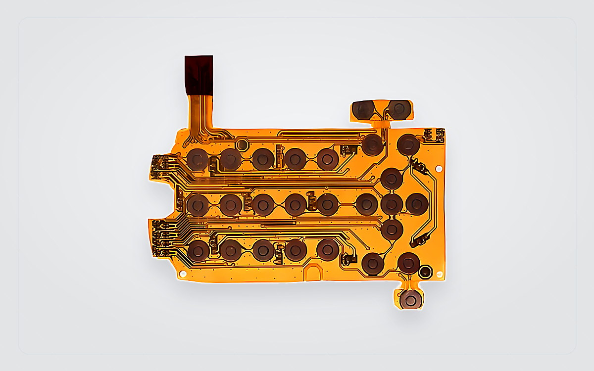
Flexible interconnect layouts with bend areas, stiffeners, connector interfaces and space limits considered.
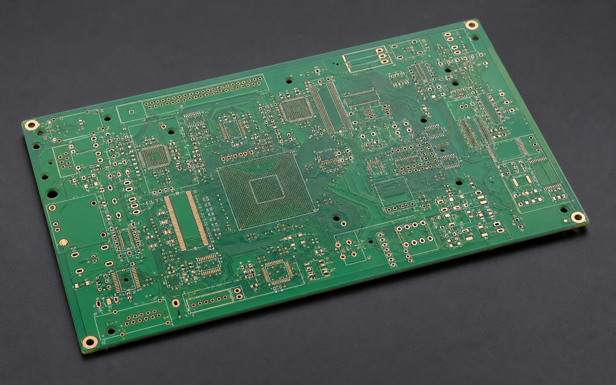
Single-layer, double-sided and multilayer layouts for industrial, control and general electronic products.
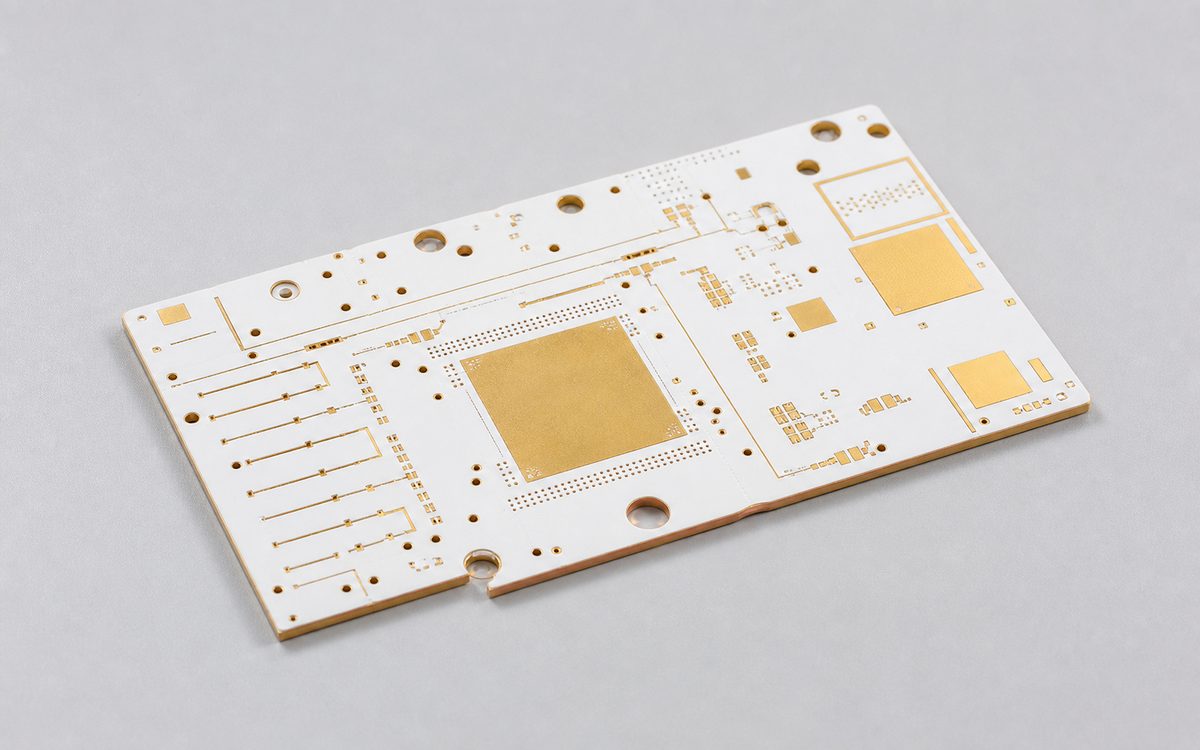
Layouts for thermal, power and high-reliability applications using ceramic substrate requirements.
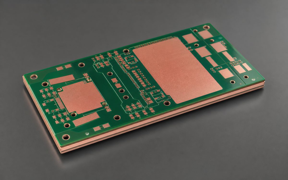
Thermal-focused layouts for LED, power conversion and other heat-sensitive electronic products.
These case studies show how placement, routing, signal integrity, and manufacturability requirements were addressed in industrial control, network switching, and high-speed interconnect projects.
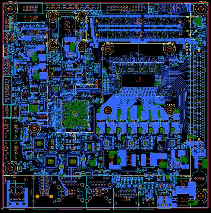
Compact industrial motherboard layout supporting multiple processor options and production interfaces.
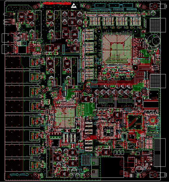
High-density network-board layout documented around switching, memory and high-current requirements.
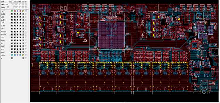
High-speed multilayer layout example for dense optical-network connectivity and controlled differential routing.
You do not need every file before contacting us. Start with the information currently available; our first review identifies what is still required.
The objective is not only to finish the layout. PCB layout, DFM and manufacturing reviews connect the released design to the intended fabrication and assembly process.

Owns placement, routing and the confirmed electrical and mechanical layout requirements.
Reviews fabrication and assembly risks before the agreed production files are released.
View the DFM evidence routeChecks that the released construction and file package align with the intended PCB and PCBA route.
Meet the engineering approachDesign revisions, review comments and released files are controlled against the approved project baseline.
Share your PCB type, available files, target schedule, and basic project requirements. You can start with non-confidential information before sending detailed design files.
The required inputs, design scope, deliverables, estimated lead time, and quotation basis are confirmed before the project starts, so you know exactly what is included.
The PCB layout is completed around the agreed requirements. Review comments and revisions are tracked before the design is finalized, reducing the risk of missed changes.
After final approval, the agreed source files, fabrication files, and assembly files are organized and delivered for your next project stage.
Send your schematic, board outline, BOM, or existing design files. We’ll check what is ready, identify anything still needed, and confirm the design scope, deliverables, and timeline before work begins.
Initial response within 12 hours. You can start with incomplete files for the first project review.