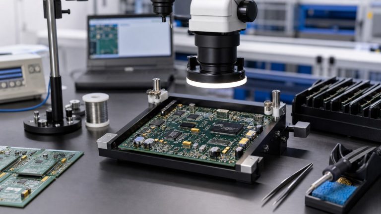
We manufacture high-reliability PCBs from an approved material system, not from a laminate trade name alone. Our engineers review the operating environment, electrical requirements, thermal exposure, via structure, copper, stack-up, assembly cycles and documentation needs before we release the construction.
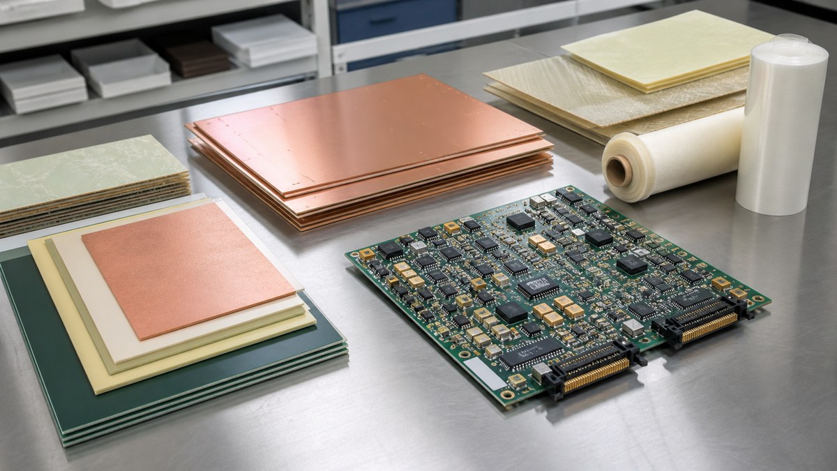
You receive a material and stack-up proposal tied to your design requirements, together with the engineering questions that must be closed before production. Where material certificates, lot identity, impedance evidence or substitution approval are required, we include those controls in the project route.
What We Review Before Approving a Material System
| Your requirement | What we review | What you receive |
|---|---|---|
| Thermal reliability | Tg, decomposition behavior, CTE, assembly cycles and via structure | Approved material and stack-up decision |
| RF or high-speed performance | Dk, Df, frequency, test method, copper profile and geometry | Controlled construction and impedance evidence plan |
| Mechanical reliability | Board thickness, copper distribution, hole structure and support conditions | Manufacturable construction and identified risks |
| Environmental exposure | Moisture, temperature, cleanliness, coating and surface requirements | Material and process controls applicable to the environment |
| Production continuity | Material availability, source, equivalent rules and change approval | Released material baseline and substitution boundary |
| Qualification evidence | Required certificate, lot, coupon, test or inspection record | Agreed evidence package for the build |
We Start With the Product Environment
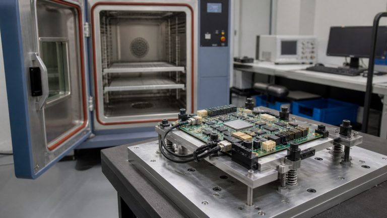
Our review begins with the conditions the PCB must survive: operating and storage temperature, thermal cycling, vibration, humidity, altitude, voltage, current, frequency, assembly profile and expected service life. A material that is suitable for one aerospace assembly may be unsuitable for another when the via structure, heat exposure or RF requirement changes.
We ask for the actual requirement instead of automatically recommending the highest-cost laminate. A higher Tg value alone does not prove better reliability, and an RF laminate is unnecessary when the electrical design does not need its properties. The correct choice is the material system that meets the defined risks and remains controllable in production.
Thermal Properties Must Match the Via Structure
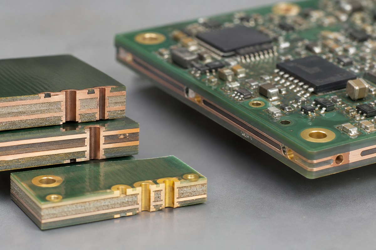
We review Tg together with decomposition behavior, through-thickness CTE, board thickness, plated-hole aspect ratio, microvia construction and the number of assembly thermal cycles. This matters because a laminate label cannot predict plated-hole reliability without the finished PCB structure.
Where the design uses sequential lamination, stacked or staggered microvias, heavy copper or repeated assembly exposure, we identify the construction and process questions before release. You receive a clear record of the approved stack-up, material callout and any qualification or inspection evidence required for the structure.
Electrical Properties Are Reviewed at the Relevant Frequency
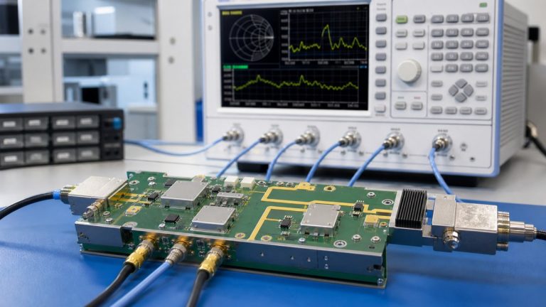
For controlled-impedance, high-speed or RF designs, we review dielectric constant and dissipation factor in the context of frequency and test method. Datasheet values produced by different methods are not automatically interchangeable. Copper profile, resin content, dielectric thickness, solder mask and trace geometry also influence the manufactured result.
Our fabrication review connects the selected material to the proposed production stack-up and controlled structures. Where impedance testing is required, we define the coupon and report basis with the released construction. Material data, geometry and measurement therefore remain connected to the same revision.
We Review the Complete Material System
The finished PCB includes more than laminate. We review prepreg, copper foil, solder mask, surface finish and any applicable coverlay, adhesive, stiffener or metal-core layer. Their compatibility affects fabrication, assembly, electrical behavior, moisture response and mechanical reliability.
For rigid-flex designs, we also separate static and dynamic bend requirements and review the transition between rigid and flexible regions. For high-current designs, copper distribution and resin fill can affect manufacturability and flatness. These decisions are recorded in the approved construction rather than left as purchasing substitutions.
Material Availability Is Part of Reliability
A technically suitable material cannot support repeat production if its exact grade, construction or source is unavailable. We review availability and approved-source requirements before release. If an equivalent is allowed, we define which properties must match and which changes require customer approval.
We do not replace a specified material only because another product has a similar Tg or brand description. Electrical, thermal, mechanical, processing and documentation differences are reviewed together. Proposed changes remain outside the production baseline until the required approval is received.
We Preserve Material Identity and Production Evidence
Where required by the project, our records can connect the approved material callout and available material identity to the production work order. The agreed evidence may include material certificates, supplier or grade information, lot records, stack-up confirmation, impedance results, microsection results or other specified inspection documents.
The evidence package is defined before production so your team knows which records will be supplied, which will be retained and which identifiers support retrieval. This turns “high-reliability material” from a marketing phrase into a controlled construction with reviewable evidence.
Why Customers Use Our Material Review
We help customers avoid two costly mistakes: selecting a material from one datasheet value, and over-specifying an expensive material without connecting it to a real product risk. Our engineers compare the operating requirement with the complete PCB construction and the production controls needed to maintain it.
You receive an approved material baseline, resolved engineering questions and an evidence plan suitable for the project. This supports prototype learning, repeat orders and controlled material changes without silently altering the design intent.
Send the Inputs for a High-Reliability Material Review
Send your Gerber or ODB++ data, stack-up, fabrication drawing, board thickness, copper, via structure, impedance targets, operating and storage temperatures, thermal-cycle requirement, frequency, assembly profile, quantity, approved-material restrictions and required certificates or reports to sales@ebestpcba.com.
Our engineers will return the material questions, proposed manufacturing construction, evidence available for the build and any item that requires your approval before production.