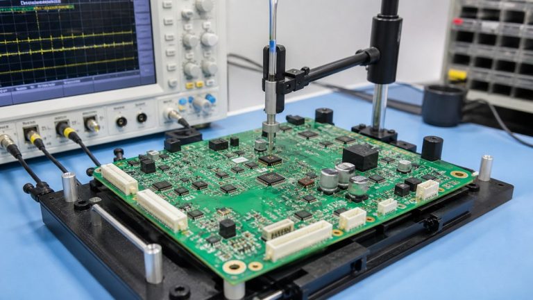
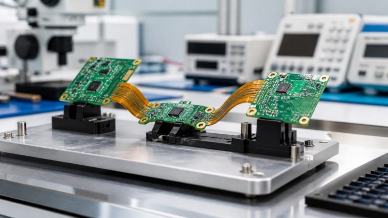
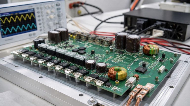
We manufacture machine-vision and sensor PCBs from an approved stack-up, material system and controlled high-speed geometry. Our engineers connect differential pairs, reference planes, vias, connector launches and impedance requirements to the actual fabrication construction before CAM release.
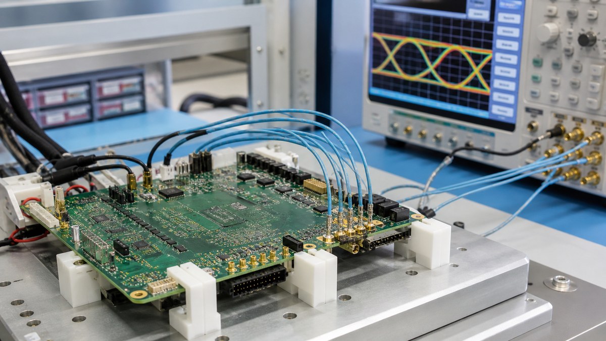
You receive a proposed production stack-up, engineering questions and applicable impedance evidence tied to the released revision. We do not redesign your interface or claim system performance; we prevent manufacturing substitutions and geometry changes from silently altering the validated signal path.
Signal-Integrity Manufacturing Map
| Critical item | Our control | Evidence |
|---|---|---|
| Stack-up | Fix layer functions, dielectrics, copper and finished thickness | Approved production stack-up |
| Impedance structure | Link target, layer, reference and geometry | Controlled structure and coupon report |
| Material | Review Dk, Df, frequency, copper profile and availability | Released material baseline |
| Via transition | Control drill, plating, layer pairs and backdrill where specified | Drill and applicable inspection evidence |
| Connector launch | Preserve geometry, registration and mechanical location | DFM response and dimensional evidence |
We Start With the Interface and Frequency Requirement
We ask for interface type, data rate or relevant frequency, target impedance, tolerance, critical nets, reference layers and any insertion-loss or coupon requirement. These inputs identify which physical structures require control.
Your engineering team owns signal-integrity design and margin. We use the released requirement to establish a manufacturable construction and evidence plan.
The Production Stack-Up Remains the Electrical Basis
We review layer function, dielectric thickness, material construction, copper and total thickness together. Available cores and prepregs must create the approved relationship between traces and reference planes.
When a buildable construction requires a geometry or material change, we return the proposal for approval. The final stack-up becomes the basis for CAM, drilling, impedance modelling and coupons.
Material Data Need Frequency and Test-Method Context
Dk and Df values depend on frequency, test method and material construction. Copper roughness and resin content also influence high-speed loss. We do not select a material from a brand name or one headline value.
Our review identifies the approved grade, source or equivalent rule and how material changes will be controlled for repeat production.
We Protect Differential Geometry Through Fabrication
We review trace width, pair spacing, copper thickness, solder-mask condition, reference plane and manufacturing tolerance. Proposed compensation is returned through an engineering query when it changes the released geometry.
Representative impedance coupons are linked to the controlled structures where required. The report identifies the measured target, lot and revision.
Vias and Backdrill Stay Tied to the Final Construction
We review drill pairs, finished hole, pad, antipad, registration and remaining-stub requirement for high-speed transitions. Backdrill side and target layer must be explicit.
The applicable inspection method is agreed before release. Structural evidence can verify the manufactured feature, while system eye-diagram or link performance remains a separate customer validation.
Connector and Camera Interfaces Need Mechanical Accuracy
We check connector footprint, board edge, mounting holes, launch geometry, component keep-outs and assembly access. A small dimensional shift can affect both signal path and mechanical fit.
Approved mechanical data and critical dimensions enter the controlled package and inspection plan.
Assembly and Test Must Not Obscure the High-Speed Risk
We review fine-pitch packages, BGAs, shielding, grounding hardware and rework access. SPI, AOI and X-ray are assigned according to visible and hidden assembly risks.
Customer-defined interface or functional testing uses the approved firmware, fixture, cable, data condition and limits. An impedance coupon and a powered link test prove different parts of the product.
Why Machine-Vision Customers Use Our Control Route
We keep material, stack-up, geometry, via construction and evidence connected to one revision. Your engineers can see how the validated physical design enters manufacturing and what was measured after fabrication.
This reduces construction drift across prototypes and repeat orders.
Send Your Machine-Vision PCB Data
Send product files, stack-up, material requirement, copper, impedance table, critical nets, interface or frequency information, via and backdrill details, connector mechanical data, quantities and test-report needs to sales@ebestpcba.com.
We will return the proposed construction, manufacturing questions and evidence plan.