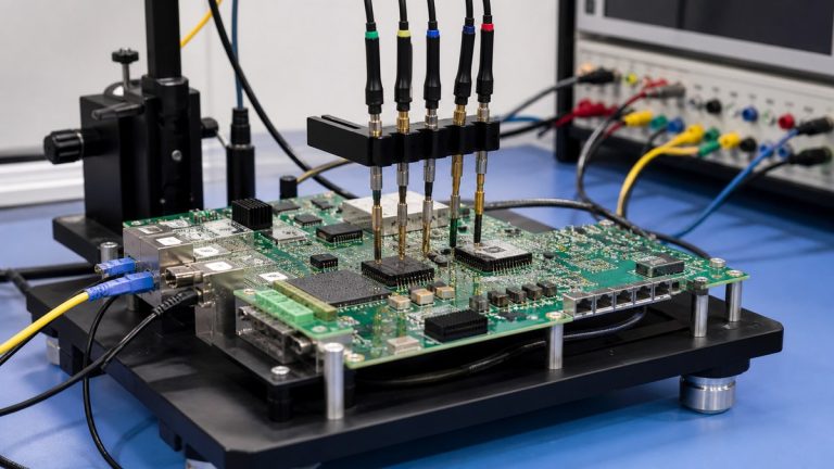
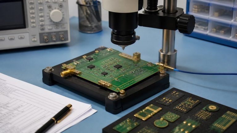
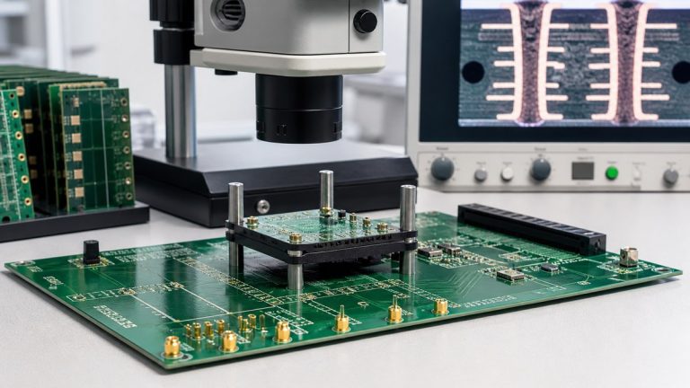
We manufacture high-speed PCBs from one approved electrical and physical construction. Our engineers connect stack-up, material, copper, impedance geometry, reference planes, vias, backdrill, connectors and test coupons before CAM release.
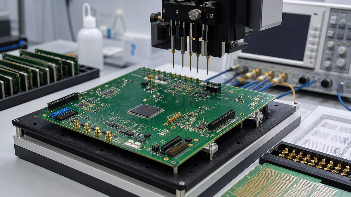
You receive a controlled production stack-up, resolved engineering questions and applicable fabrication evidence tied to the released revision. We preserve your signal-integrity design intent while preventing material or geometry decisions from drifting between prototype and repeat production.
High-Speed Production Baseline
| Design item | Our control | Evidence |
|---|---|---|
| Layer structure | Fix layer functions, dielectric, copper and finished thickness | Approved production stack-up |
| Impedance | Link target, layer, reference, width and spacing | Controlled structures and coupon report |
| Material | Review Dk, Df, frequency, copper profile and source | Released material baseline |
| Via transition | Control drill pairs, plating and backdrill where specified | Applicable structural evidence |
| Repeat order | Compare requested build with approved construction | Change review and lot records |
We Reconcile the Electrical and Manufacturing Files
We compare Gerber or ODB++, drill data, stack-up, fabrication drawing, impedance table, material requirement and mechanical information. Critical nets, reference layers and via structures must describe the same revision.
Conflicts become engineering questions before production data are generated. Approved responses remain with the released package.
The Production Stack-Up Controls the Physical Channel
We build the layer structure from available cores, prepregs, copper and material construction while preserving approved dielectric relationships. Finished thickness, resin content and copper distribution are reviewed together.
If a manufacturable build requires a change, we return the proposed construction and affected geometry for customer approval.
We Control Impedance Geometry Through CAM
Target impedance must identify single-ended or differential condition, layer, reference, relevant nets and tolerance. We model production width, spacing, copper, dielectric and mask condition from the approved stack-up.
Manufacturing compensation that changes the released geometry follows the agreed engineering-query route rather than being introduced silently.
Materials Stay Connected to the Approved Basis
We review Dk and Df with frequency and test method, together with copper profile, thermal behavior and availability. A trade name alone does not define the exact construction.
Material substitutions are evaluated for electrical, mechanical and process effects and require the agreed approval before repeat production.
Vias and Backdrill Follow the Final Stack-Up
We review drill side, layer pair, hole and pad geometry, antipads, registration, backdrill depth and remaining-stub requirement. These details cannot be finalized independently of the production stack-up.
Applicable inspection evidence verifies the manufactured structure. Link performance remains a separate customer validation.
Coupons Provide Defined Fabrication Evidence
Where impedance testing is required, we place representative coupon structures on the production panel and connect them to their target, layer and reference. The report identifies the lot and revision.
A coupon demonstrates its measured structure under the stated conditions. It does not prove every routed channel, connector or complete system margin.
Assembly Risks Remain Part of High-Speed Production
We review fine-pitch packages, BGAs, connectors, shields, grounding hardware and rework access. SPI, AOI and X-ray are assigned according to visible and hidden-joint risks.
Customer-defined interface testing uses approved hardware, firmware, fixtures, cables and limits. Manufacturing and functional evidence remain clearly separated.
Repeat Orders Return to the Same Construction
We compare material, stack-up, impedance structures, drill basis and test plan with the approved baseline. Proposed changes receive engineering review before release.
Available material, work-order and report records support continuity across production lots.
Why High-Speed Customers Use Our Control Process
We connect the complete physical channel to one production package and evidence plan. Your team can see how the validated design enters fabrication and which measured result supports the manufactured construction.
This reduces prototype-to-production drift and undocumented changes in repeat orders.
Send Your High-Speed PCB Data
Send product files, stack-up, fabrication drawing, material requirement, copper, impedance table, critical-net information, via and backdrill details, connector data, quantities and report needs to sales@ebestpcba.com.
We will return the proposed production construction, open questions and evidence plan.