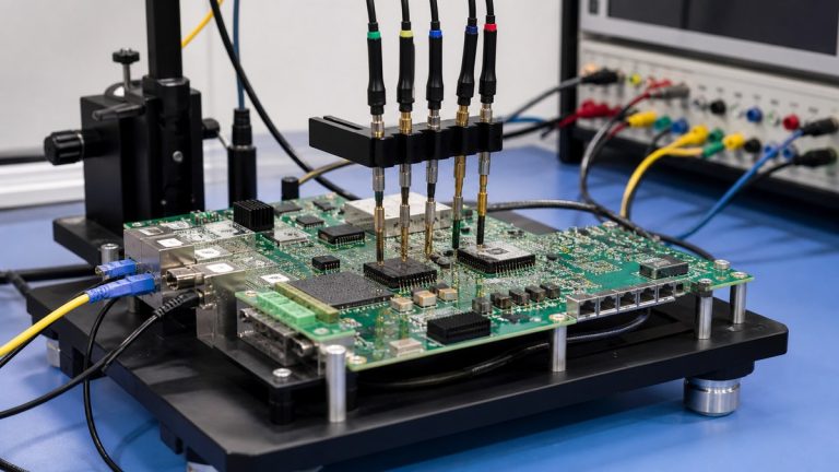
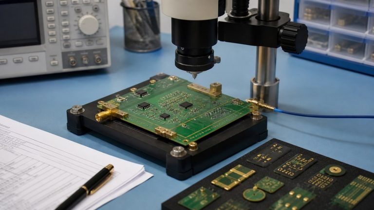
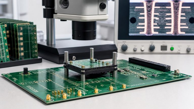
Select a low-loss PCB material from the required frequency, channel length, insertion-loss budget, impedance structure and manufacturing conditions—not from the lowest Df number on a datasheet. Copper profile, dielectric thickness, glass construction, vias, connectors, finish and assembly can contribute enough loss to change the result.
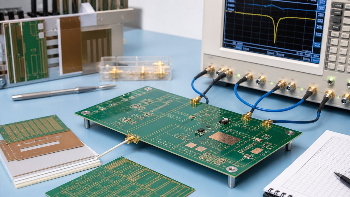
We help customers turn a validated electrical requirement into a manufacturable material and stack-up baseline. You receive a comparison of relevant properties, availability and process trade-offs, followed by an approved production construction and evidence plan.
Low-Loss Material Selection Matrix
| Question | Why it matters | Our production review |
|---|---|---|
| What frequency and loss budget apply? | Defines whether lower dielectric loss is needed | Connect requirement to material and channel structure |
| How are Dk and Df measured? | Values from different methods are not directly interchangeable | Use an approved datasheet basis |
| Which copper profile applies? | Conductor roughness affects high-frequency loss | Review foil and laminate construction |
| Is a hybrid stack-up planned? | Materials must laminate and process together | Review compatibility and controlled transitions |
| Can the material support repeat orders? | Unavailable construction creates redesign or drift | Define grade, source and substitution rules |
Start With a Real Electrical Requirement
We ask for frequency or data rate, channel length, topology, loss or eye-margin requirement, target impedance and relevant test method. A short low-speed channel may not benefit from an expensive RF laminate.
Your signal-integrity or RF team sets the performance target. We use it to review which material characteristics need manufacturing control.
Dk Needs Frequency and Test-Method Context
Dielectric constant influences impedance and propagation. Datasheet Dk values can vary with frequency, test method and material construction, so one number should not be copied blindly into every field solver.
We connect the approved design basis to the selected material and production stack-up. If a source or construction changes, the electrical effect receives review.
Df Is Only One Part of Insertion Loss
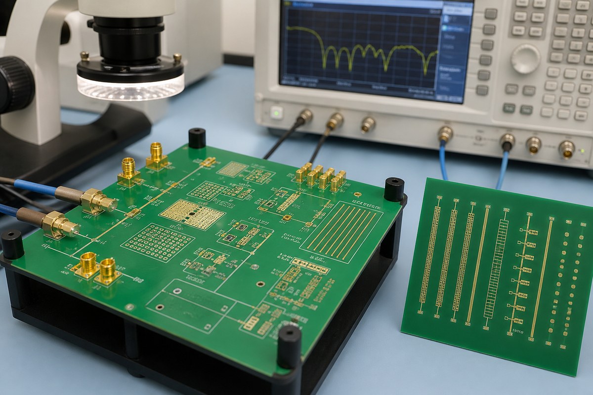
Dissipation factor describes dielectric contribution, but conductor loss, copper roughness, trace geometry, vias, connectors and finish also matter. Selecting the lowest Df cannot correct an unsuitable channel structure.
We keep the material decision connected to the complete manufactured interconnect and avoid presenting one datasheet value as a performance prove.
Copper Profile Can Change the Trade-Off
Rougher copper improves bonding in some constructions but increases conductor loss at high frequency. We review the specified or available foil with the laminate, stack-up and fabrication process.
A smoother foil choice may affect cost, availability and processing. The approved decision remains part of the material baseline.
Glass and Resin Construction Affect Local Behavior
Glass style, resin content and dielectric thickness influence the effective properties around routed traces. Stack-up design and routing placement may matter as much as the laminate family name.
Our production proposal identifies the actual core and prepreg construction used to build the board.
Hybrid Stack-Ups Need Compatibility Review
Combining low-loss and standard materials can control cost, but lamination, CTE, drilling, plating and thickness relationships must remain compatible. We review regional electrical needs and the full fabrication route.
Hybrid construction is not automatically cheaper if added complexity, yield or qualification outweighs material savings.
Assembly and Rework Still Matter
We review thermal exposure, moisture handling, surface finish, component packages and rework needs. A material selected only for RF performance may create avoidable assembly constraints.
The approved construction must support both fabricated electrical features and the intended PCBA process.
Availability and Substitution Protect Repeat Production
We confirm exact grade, construction, source and acceptable-equivalent rules. A material with excellent published data cannot support production if the required construction is unavailable or changes without review.
Proposed substitutions receive electrical, mechanical and process comparison before customer approval.
What Evidence We Can Provide
The project can define material identity, approved stack-up, impedance coupons, test reports and available lot records. These prove the manufactured construction and selected measurements.
System insertion loss, eye margin or RF performance requires the test method and responsibility agreed for the product.
Send Your Low-Loss Material Requirements
Send product files, stack-up, frequency or data rate, channel length, loss target, impedance, copper, material preferences, assembly profile, quantity, sourcing restrictions and report needs to sales@ebestpcba.com.
We will return material options, manufacturing trade-offs, the proposed construction and evidence plan.