We manufacture backdrilled PCBs from the final approved stack-up, explicit drill pairs and a measurable remaining-stub requirement. Our engineers convert the customer’s signal-integrity instruction into controlled drill side, diameter, depth, registration, clearance and inspection data.
You receive DFM questions, an approved backdrill basis and the structural evidence defined for the project. We do not choose the electrical stub limit for the customer; we show whether the specified result is manufacturable and how it will be verified.
Backdrill Control Matrix
| Input | Our control | Evidence |
|---|---|---|
| Via identity | Identify exact vias and applicable nets or classes | Released backdrill data |
| Drill side and layer pair | Reference the final stack-up | Approved depth basis |
| Backdrill diameter | Review primary hole, annular ring and antipad clearance | DFM response |
| Remaining stub | Account for layer location and process tolerance | Applicable microsection or depth evidence |
| Repeat order | Protect the same stack-up and drill basis | Controlled revision history |
We Start With Explicit Via and Layer Information
The released package must identify which vias require backdrill, from which side and to which target layer. Top-to-bottom language alone is not enough when stack-up revisions can change layer numbering.
We reconcile drill files, drawings, net classes and stack-up before programming. Conflicts return for customer approval.
The Final Stack-Up Controls the Depth Calculation
Core, prepreg, copper and finished thickness determine the physical location of every layer. Backdrill depth cannot be finalized from an early or nominal stack-up.
We release drilling only after the production construction is approved. Material or thickness changes trigger review of the depth basis.
Diameter Must Protect Pads and Adjacent Features
We compare the primary plated hole with the backdrill diameter, pad, antipad, adjacent copper and registration tolerance. A larger backdrill removes more residual barrel but also consumes more clearance.
If the geometry cannot support both the stub and clearance requirement, we return the trade-off before fabrication.
Remaining Stub Is a Tolerance-Controlled Result
The specified maximum stub must account for actual layer position, board thickness variation, drill depth tolerance and measurement method. We identify the reference point and acceptance basis used by production and inspection.
A nominal depth without a measurable result does not provide reliable control.
Primary Drilling and Plating Still Matter
Backdrill removes unused barrel but does not correct poor primary drilling, plating or registration. We keep the original via structure and applicable PCB controls visible in the process plan.
Electrical test confirms connectivity and isolation; structural inspection answers the physical stub and drilling question.
Inspection Matches the Approved Requirement
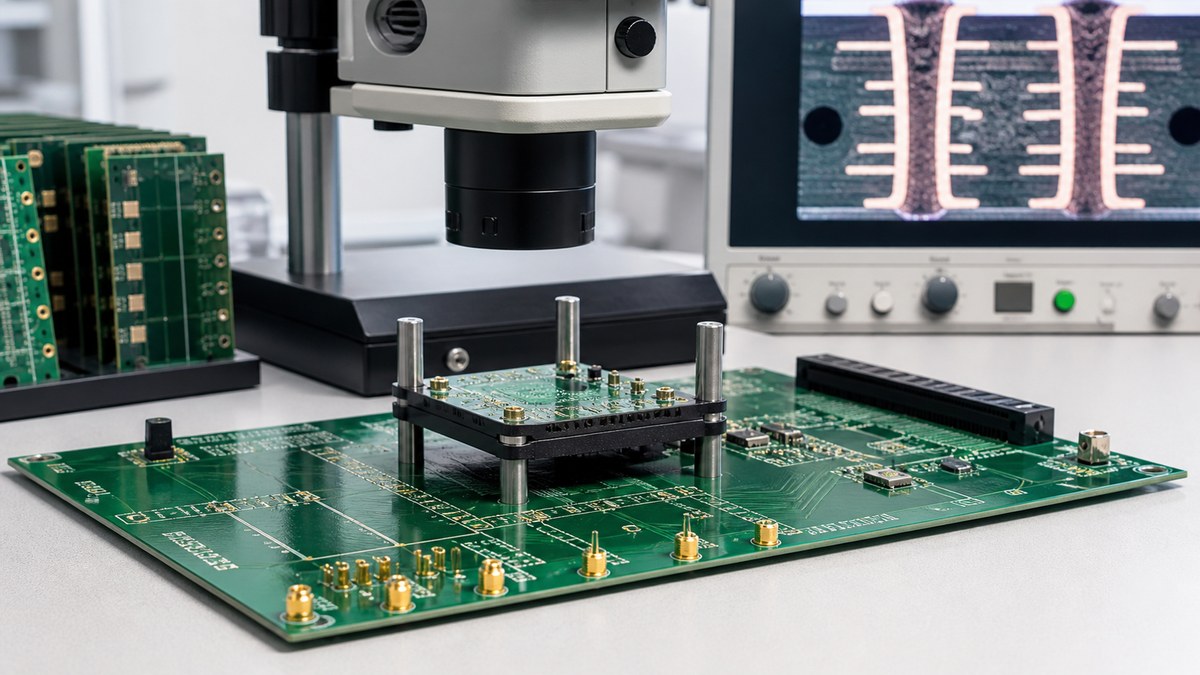
The evidence may include selected microsection, depth, dimensional or other approved structural verification. The plan defines sample location, representation, acceptance and report needs.
We connect the result to the lot and revision. A coupon or sample only proves the structure it represents under the agreed plan.
Failures Receive Lot-Level Disposition
If backdrill evidence does not meet the requirement, affected product is contained and reviewed. We do not silently relax the stub limit or ship based on electrical continuity alone.
The disposition, additional inspection or customer decision remains recorded.
Why High-Speed Customers Use Our Backdrill Process
We link the electrical requirement to an explicit physical feature, final stack-up and measurable inspection. Your team can review the real drill basis rather than a generic statement that the board was backdrilled.
This protects high-speed construction across first builds and repeats.
Send Your Backdrill Requirements
Send Gerber or ODB++, drill files, final stack-up, via list or classes, drill side, target layer, primary and backdrill diameters, remaining-stub limit, clearance rules, quantity, sampling and report needs to sales@ebestpcba.com.
We will return DFM questions, the controlled drill basis and inspection plan.
What We Need to Review a Backdrill Requirement
Provide the final stack-up, plated drill table, backdrill pairs, drill side, target remaining stub, relevant nets and any keep-out constraints. We will check tool access, registration allowance, clearances and a practical verification method. You receive questions before release and can approve the exact construction that our fabrication and inspection teams will follow.