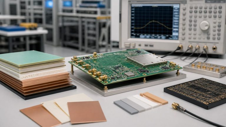
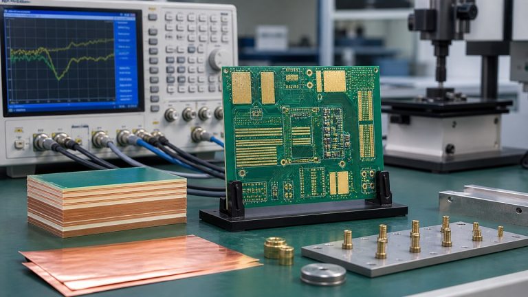
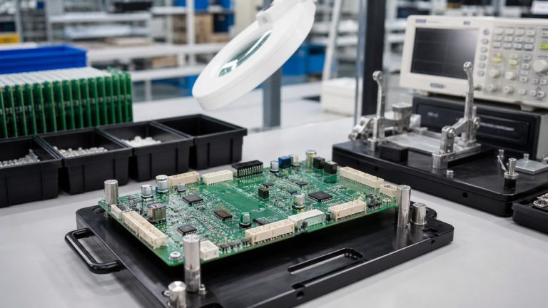
Select a PCB or PCBA test from the failure question you need to answer. Bare-board electrical testing checks connectivity before assembly; AOI and X-ray inspect physical assembly conditions; ICT and flying probe check accessible electrical conditions; functional testing verifies specified powered behavior.
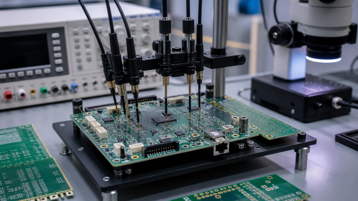
We build project test routes by connecting the released product, method, program or procedure, acceptance criteria and report. The comparison below helps you avoid expecting one test to cover every risk.
PCB and PCBA Test Comparison
| Method | Best used for | Main boundary |
|---|---|---|
| Bare-board electrical test | PCB continuity and isolation | No component or functional coverage |
| Impedance coupon test | Defined controlled structures | Does not prove the complete channel |
| AOI | Visible placement and solder conditions | Cannot see hidden joints or function |
| X-ray | Selected hidden interconnects | Does not prove powered behavior |
| ICT/flying probe | Accessible connectivity and component conditions | Coverage depends on design access |
| FCT | Specified powered inputs, outputs and interfaces | Only proves defined conditions |
Bare-Board Electrical Test Checks the Fabricated Network
Electrical testing compares the PCB with released net data to identify applicable opens and shorts. Fixture testing can suit stable repeat volume, while flying-probe methods provide flexibility for prototypes and changing designs.
Thresholds, test voltage and report requirements should be defined when they are customer-specific. A passed bare board says nothing about later component assembly.
Impedance Testing Measures Defined Coupon Structures
Controlled-impedance testing uses coupons designed from the approved stack-up and geometry. The report identifies target, result, lot and revision.
Coupon evidence does not automatically cover every routed trace, via, connector or complete high-speed channel.
SPI Monitors Solder Paste Before Placement
SPI can check applicable paste volume, area, height and alignment before components hide the deposits. It provides an upstream process signal for stencil printing.
Reaction rules are necessary; collecting data without correcting the process does not reduce risk.
AOI Covers Visible Assembly Conditions
AOI checks applicable component presence, position, polarity and visible solder conditions. Programs follow the released product and approved workmanship basis.
AOI cannot reliably inspect hidden BGA or QFN joints and does not prove electrical function.
X-ray Supports Selected Hidden-Joint Inspection
X-ray is useful for BGA, QFN, exposed-pad and other bottom-terminated structures. Coverage, sampling, acceptance and image output need a product-specific plan.
It should be combined with process and electrical methods when those answer different questions.
ICT and Flying Probe Depend on Test Access
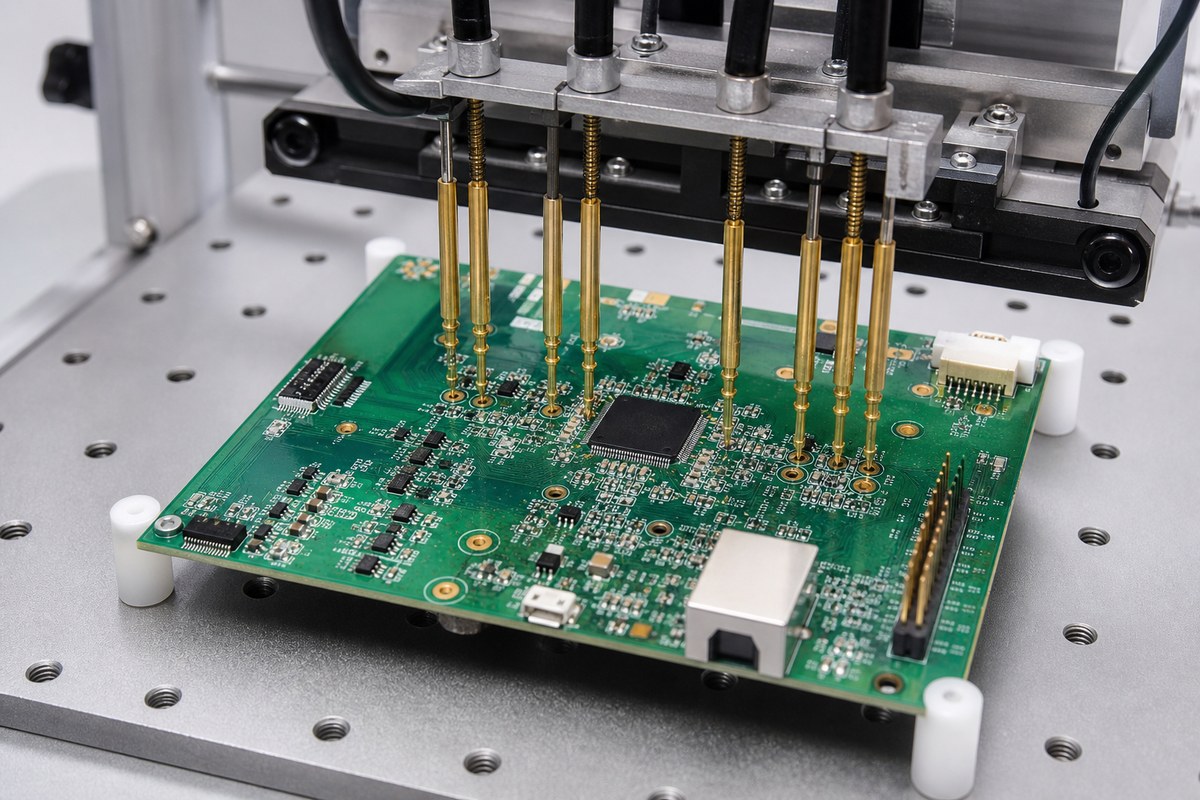
These methods can check defined connections and components when the PCB provides suitable access. Fixture, probes, isolation, program, limits and expected volume affect the choice.
The report should state coverage and disposition instead of implying complete function.
Functional Testing Verifies Specified Behavior
FCT powers the assembly and checks defined inputs, outputs, communication or control functions. It requires fixtures, firmware, procedures, loads, limits and expected results.
A simple power-on check is not equivalent to full function, environmental, safety or lifetime validation.
Environmental and Reliability Tests Are Separate Scopes
Thermal cycling, vibration, humidity, burn-in and endurance tests require representative conditions, samples, duration and acceptance. They are not automatically included in standard PCBA functional testing.
We can align manufacturing samples and records with an agreed customer or external qualification plan.
Failures, Repairs and Retests Need One Evidence Chain
A useful record keeps the initial failure, diagnosis, approved repair or rework, retest and final disposition visible. Product or serial links improve later retrieval.
A final pass field alone can hide recurring process or fixture problems.
How We Build Your Test Proposal
We review product risk, package mix, access, volume, firmware, functions, customer standards and report needs. Then we assign each risk to prevention, inspection or test and identify uncovered conditions.
You receive a coverage map explaining what each method proves, the required inputs and the evidence available.
Send Your PCB or PCBA Test Requirements
Send product files, netlist, BOM, CPL, assembly drawing, test points, firmware, procedure, fixture information, loads, limits, golden sample, quantities, sampling and report format to sales@ebestpcba.com.
We will return the recommended method combination, coverage boundaries and evidence plan.