High-Frequency PCB Material Engineering
High-frequency circuit performance depends on a complete interconnect: material, stack-up, copper, trace geometry, vias, launches, finish and assembly. We help customers turn the validated electrical design into a manufacturable construction and documented production route. We do not select RF performance from a material brand alone.
Frequency and loss budget define the material problem
The customer provides operating frequency, bandwidth, route length, insertion-loss target, impedance and critical RF structures. This shows where dielectric and conductor loss matter.
System antennas, cables, connectors and enclosure effects remain part of customer validation.
Dk needs a frequency and test-method context
Published dielectric constant can vary with method, frequency, resin and glass construction. The value used in circuit simulation should be identified with its source.
EBest aligns the manufacturing proposal with the approved basis and avoids representing a nominal value as a measurement of every finished board.
Df is one contributor to insertion loss
Dissipation factor helps compare dielectric loss under stated conditions, but total channel loss also includes copper, geometry, vias, launches and connectors.
A lower Df does not automatically justify a more difficult or unavailable construction if the system budget does not require it.
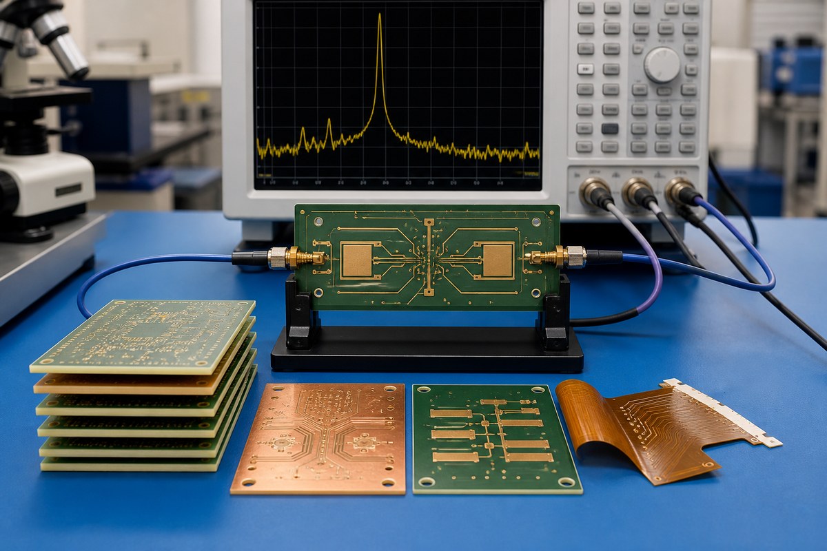
Copper foil profile influences conductor loss
Copper surface condition, foil type and finished thickness may influence high-frequency behavior and bonding. The customer specifies an approved foil or roughness requirement where it matters.
Substitution follows controlled review because similar laminate with different copper may not match the validated model.
Glass and resin construction affect local properties
Glass weave, resin content and dielectric thickness can influence consistency and routing behavior. Critical requirements should be expressed through approved construction or measurable limits.
EBest confirms the production build within the agreed evidence scope.
Stack-up turns material properties into transmission lines
Layer order, dielectric, copper, trace width, spacing and reference planes define microstrip, stripline or coplanar structures. Our engineers review manufacturability and propose production geometry where needed.
Customer approval keeps simulation and production aligned.
Hybrid material systems require compatibility review
Combining RF and other laminates may reduce cost or meet mechanical needs, but bonding, expansion, flow and lamination cycles must work together.
The hybrid construction is controlled as a specific stack-up, not treated as interchangeable with a homogeneous board.
Vias and backdrill are part of the RF path
Signal and ground vias, layer transitions, pad/anti-pad geometry and remaining stubs can affect the channel. The customer defines electrical requirements and EBest checks drill, registration and structural manufacturability.
Backdrill evidence needs explicit layer pairs, depth and inspection.
Surface finish and solder mask need electrical context
Finish and mask conditions can affect exposed RF conductors, connectors and controlled geometry. The customer identifies critical no-mask areas, contact finish and any thickness requirement.
Fabrication and assembly handling protect those released surfaces.
Material availability affects production continuity
Prototype stock does not prove repeat supply. We identify approved manufacturer, construction and alternative boundaries during quotation.
A proposed replacement includes available property and process differences for customer review and any required RF revalidation.
Thermal behavior still matters in an RF material choice
Power amplifiers, filters and dense RF assemblies can create local heat. Material thermal properties, copper distribution, via structures and the chassis interface affect the manufactured heat path.
We review fabrication and assembly compatibility. Junction temperature and system cooling remain customer calculations and tests.
Assembly cycles and rework can influence the material system
The chosen laminate, hybrid bonding and surface finish must tolerate the proposed soldering route within approved limits. Large thermal masses or repeated rework may justify additional review or sample evidence.
We do not assume an RF data sheet alone proves compatibility with every PCBA process.
Impedance and loss reports prove different things
Impedance coupons measure defined transmission-line structures. Loss coupons or test vehicles require their own geometry, fixtures, calibration, frequency and limits. A functional RF test has another scope again.
EBest states which report is included and the boundary of its evidence.
High-frequency material decision matrix
| Design need | Material/construction question | EBest output |
|---|---|---|
| Impedance control | Are Dk basis and stack-up defined? | Geometry and coupon proposal |
| Low insertion loss | Which dielectric and copper losses matter? | Manufacturable approved material options |
| Complex RF transitions | Are via and launch structures complete? | DFM and structural evidence plan |
| Hybrid build | Are materials compatible in lamination? | Specific controlled stack-up |
| Repeat supply | Are alternatives authorized and validated? | Material identity and change boundary |
Production evidence remains traceable
Within the agreed scope, the work order can connect to the approved stack-up, available material identity, coupon result, structural inspection and final revision. Repeat lots recheck changes before use.
Reports are delivered and retained according to the project requirement.
Inputs for an EBest high-frequency review
- PCB data, drawing and proposed stack-up.
- Frequency, bandwidth and loss budget.
- Impedance targets and critical structures.
- Approved laminate, glass and copper requirements.
- Hybrid-material and lamination constraints.
- Via, backdrill, connector and finish data.
- Impedance, loss or RF test methods and limits.
- Volume, approved alternatives and change rules.
What EBest returns
Our engineers can return a material and stack-up review, manufacturable options, geometry and via questions, coupon/test evidence plan and repeat-order change boundary. Send the electrical model assumptions with the fabrication files so the chosen material supports the validated RF circuit and a stable production route.
Discuss Your Project With Our Engineers
Send us your frequency range, validated material or performance requirements, stack-up, impedance targets and RF geometry. We will review how to preserve that intent in manufacturing.
Email sales@ebestpcba.com with the current revision and expected quantity.
For your high-frequency board, we will confirm the material system, controlled geometry and evidence plan before release. You can review each manufacturing decision against your validated RF requirements and product revision.