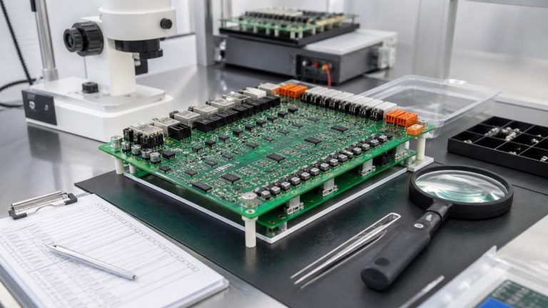
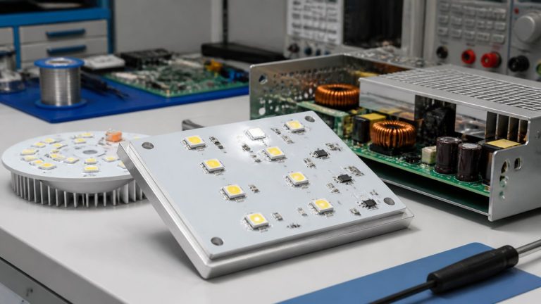
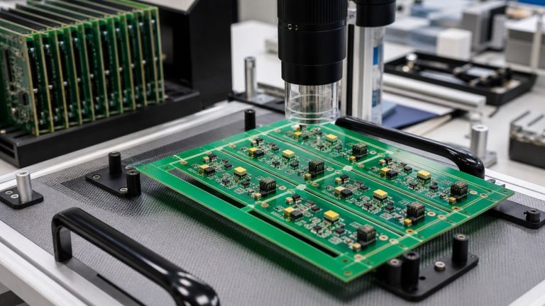
We manufacture heavy copper PCBs from layer-specific copper definitions, buildable trace and spacing rules, controlled plated structures and an assembly route matched to the board’s thermal mass. Our engineers review the current path, heat path and finished construction before production release.
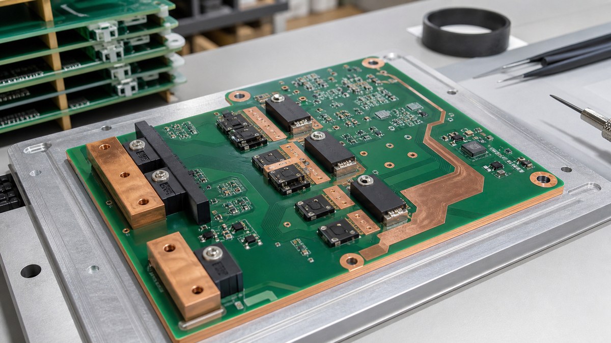
You receive an approved stack-up, DFM response and evidence plan for the critical copper and structural features. We do not recommend heavier copper automatically; it helps appropriate current and thermal designs but can reduce fine-feature capability, increase resin and flatness challenges, complicate soldering and add cost.
Heavy Copper Decision and Evidence Map
| Requirement | Our control | Evidence |
|---|---|---|
| Copper thickness | Separate starting foil, plated contribution and finished value by layer | Approved stack-up |
| Trace and spacing | Review geometry against copper and etching capability | DFM response |
| Interlayer current | Control vias, holes, annular rings and plating | Drill and applicable microsection evidence |
| Thermal interface | Review exposed pads, via arrays, heat sinks and flatness | Process and inspection result |
| Assembly | Plan stencil, soldering, fixtures and inspection for thermal mass | Controlled route and quality records |
We Start With Current and Temperature Requirements
We ask for continuous and peak current, duty cycle, allowable temperature rise, cooling path, ambient condition and qualification basis. These inputs explain where thick copper is needed and where ordinary copper may be sufficient.
Your design team sizes the conductor and validates operating temperature. We translate the approved requirement into a manufacturable PCB construction.
Copper Must Be Defined by Layer and Finished Condition
“2 oz” or “heavy copper” is incomplete when the layer, starting foil and finished requirement are unclear. We reconcile the stack-up, fabrication drawing and Gerber data before quotation and CAM release.
Different layers may need different copper. The final construction also accounts for plating, dielectric thickness and total board thickness.
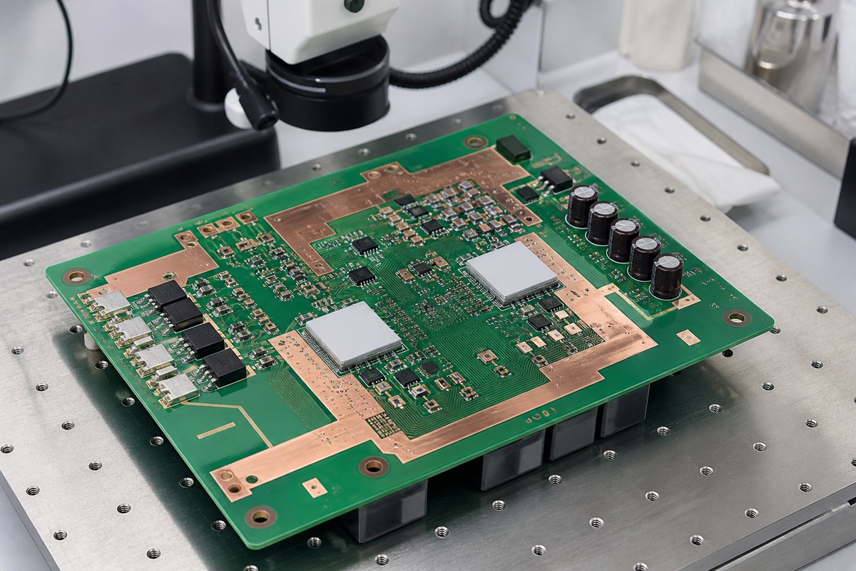
Thicker Copper Changes Trace and Spacing Capability
Deeper etching makes fine lines and tight gaps more difficult. We compare actual minimum geometry with the requested copper and return conflicts before production.
Where fine-pitch routing and high current coexist, a selective layer strategy or other design decision may be more practical than increasing every layer.
Resin Fill, Copper Balance and Flatness Need Review
Large copper steps and uneven distribution influence lamination, resin fill, thickness and board flatness. We review copper balance, dielectric construction, board size and panel strategy.
The approved stack-up records the build rather than leaving the fabricator to choose an undocumented compensation.
Vias and Plated Holes Complete the Current Path
We review finished holes, aspect ratio, plating requirement, via quantity, annular ring and connection to planes. A wide surface trace does not solve an undefined interlayer bottleneck.
Where required, microsection or other structural evidence verifies representative plated features. Electrical current validation remains tied to the complete design.
Heavy Copper Changes PCBA Soldering
High thermal mass affects paste, preheat, reflow, selective soldering, manual soldering and rework. We review power terminals, exposed pads, connectors and large components with the intended production construction.
Fixtures, stencil decisions and inspection coverage are established from the actual board rather than a lighter prototype.
Inspection Proves the Manufactured Feature
Applicable dimensional, structural, SPI, AOI or X-ray evidence can verify copper-related construction and assembly conditions. We define the feature, acceptance and record before production.
These results do not replace full-load or system thermal testing. We state the boundary so your team receives evidence that is useful and correctly interpreted.
Why Customers Use Our Heavy Copper Process
We connect current and thermal intent to buildable copper, plated connections, lamination and assembly controls. Your team can see the trade-offs and approve the final construction before material is committed.
This avoids paying for unnecessary copper or discovering too late that fine features and soldering cannot support the selected thickness.
Send Your Heavy Copper PCB for Review
Send Gerber or ODB++, stack-up, layer copper, finished-thickness definitions, trace and spacing, current, duty cycle, temperature conditions, via requirements, BOM, assembly drawing, quantities and evidence needs to sales@ebestpcba.com.
We will return the proposed construction, DFM issues and manufacturing evidence plan.