Heavy Copper PCB Quotation
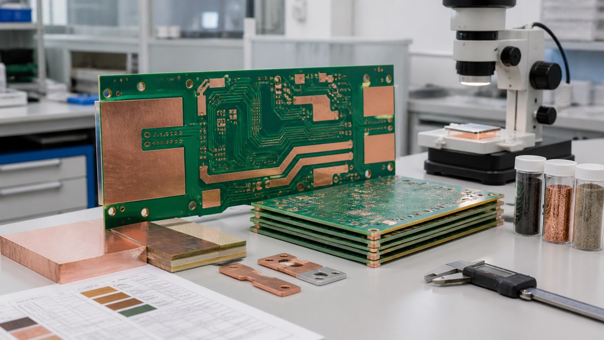
“Heavy copper” is not enough information for a reliable quotation. Copper may be described as starting foil, finished thickness or a weight, and different layers may need different values. Geometry, plating, dielectric, holes and assembly thermal mass also change the process. We ask for the engineering inputs that define the construction and the evidence the customer expects.
State whether copper is starting or finished
Base foil and plated finished copper are not the same. The fabrication drawing and stack-up should identify the required condition by layer. If copper weight is used, confirm how it relates to the finished requirement.
Our quotation states the interpreted construction so the customer can approve it before release.
Identify layers that carry the heavy copper
Outer, inner or all layers may have different copper. Layer order, dielectric and total thickness must be supplied as one stack-up.
A general note applied to a multilayer board can create unnecessary cost or an incorrect build if the actual layer requirement is not clear.
Send the real minimum trace and spacing
Etching thick copper makes very fine geometry more difficult. We review the smallest width, gap, annular features and dense locations against the proposed process.
If a change is needed, EBest identifies the affected geometry and returns a manufacturable option for electrical approval.
Current and thermal context explain the requirement
Provide continuous and peak current, duty cycle, acceptable temperature rise, ambient and cooling where available. This helps our engineers distinguish critical paths and review the assembly route.
The customer validates current capacity and temperature. Copper thickness alone is not a performance prove.
Via and plated-hole requirements need full definitions
High-current vias may require finished-hole, plating, quantity, pitch, connection and fill or cap details. Through-hole terminals add solder and mechanical constraints.
Our review confirms manufacturability and applicable inspection without recalculating the customer’s electrical design.
Dielectric and resin fill must suit the copper distribution
Heavy inner copper creates deeper features for lamination. Material, prepreg, resin behavior, copper balance and finished thickness need a compatible construction.
Approved material alternatives are stated because a material change may affect both fabrication and electrical behavior.
Surface finish and mask geometry remain important
Finish, mask openings, exposed copper and large pads influence solderability and assembly. Fine mask dams may not be compatible with heavy-copper geometry.
Any contact, bus or edge-plating requirement should be included in the drawing.
Assembly thermal mass affects tooling and process
Large planes, power devices, inductors and terminals can create uneven heating. We review stencil, support, profiling, reflow, selective or hand soldering and inspection access.
If EBest is assembling the board, provide the BOM, centroid and mechanical hardware data with the PCB RFQ.
Inspection needs a stated target
Fabrication evidence may include applicable copper, hole, dimensional, electrical or structural checks. Assembly may use SPI, AOI, X-ray or solder-fill inspection according to the risk.
Sampling, locations, acceptance and report format must be agreed before production.
Prototype evidence should support repeat production
A pilot can confirm fabrication geometry, board flatness, assembly profile and critical joints. Any adjustment is documented and transferred into the approved construction or work instruction.
One prototype board is not treated as evidence for a different stack-up or material.
Finished thickness and tolerance deserve separate attention
Heavy copper contributes to total thickness and can affect tolerance, connector fit and mechanical assembly. The drawing should identify overall thickness, local interface dimensions and any region with special control.
We review the proposed stack-up against those limits and returns conflicts before lamination.
Board size and copper balance influence flatness
Large boards or uneven copper distribution can increase distortion risk during fabrication and soldering. We review panel orientation, copper balance, support and the customer’s flatness requirement where applicable.
The measurement method and product condition need definition because bare-board and assembled flatness are different states.
Change control protects the quoted construction
A later material, copper, geometry, plating or panel change can invalidate the original quotation and process evidence. EBest identifies the change and assesses required new samples, sections, profiles or assembly checks.
Repeat orders use the approved construction rather than an assumed “equivalent” heavy-copper process.
Heavy-copper RFQ matrix
| Required input | Why EBest needs it | Quotation output |
|---|---|---|
| Layer-by-layer finished copper | Defines fabrication process | Confirmed construction |
| Minimum geometry | Determines etch capability | DFM questions or approved option |
| Via and terminal data | Sets drilling, plating and solder route | Process and inspection scope |
| Current and thermal context | Identifies critical manufacturing features | Assembly-risk review |
| Evidence requirement | Plans sampling and reports | Included records and boundaries |
Heavy-copper RFQ checklist
- Gerber or ODB++ and drill data.
- Fabrication drawing and complete stack-up.
- Starting or finished copper by layer.
- Minimum trace, gap and tolerances.
- Material and finished thickness.
- Via, plating, fill and terminal requirements.
- Current, thermal and cooling context.
- Assembly and inspection/test requirements.
What EBest returns
Our PCB and PCBA engineers can return a construction interpretation, capability questions, stack-up and geometry proposal, assembly thermal-risk review, inspection plan and evidence availability. Providing these inputs with the RFQ produces a price and process tied to the real heavy-copper board.
Discuss Your Project With Our Engineers
Send us your layer stack, finished copper by layer, current requirement, Gerber data, drawing and quantity. We will review the heavy-copper construction and return quotation assumptions for your approval.
Email sales@ebestpcba.com with the current revision and expected quantity.
For your heavy-copper project, we will confirm finished copper, geometry, plating and inspection scope before release. You can review those decisions against the quoted construction and the exact board revision.