PCB Construction Engineering
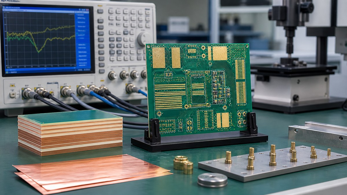
A stack-up is the manufacturing definition behind routing, reference planes, impedance, thickness and many via structures. We review the customer’s electrical target together with available material and fabrication capability, then returns a controlled construction and evidence plan. The customer owns signal-integrity design and approves any geometry or material change.
The stack-up starts with layer function
Identify signal, plane, power and mixed-function layers and the reference for critical routes. Layer order should support the validated design, not be rearranged as a routine fabrication choice.
We compare image data, drawing and stack-up names before release.
Finished thickness needs a buildable tolerance
Core, prepreg, copper and plating combine into the finished board. Connector fit, enclosure and controlled structures may depend on total or local thickness.
EBest proposes a build within the supplied requirement and returns conflicts before lamination.
Copper definitions must distinguish base and finished values
Outer-layer plating changes finished copper, while inner layers follow a different process. The drawing should identify the intended value by layer.
Copper affects impedance geometry, current paths and etching capability, so ambiguous weight labels are clarified.
Material properties need an approved basis
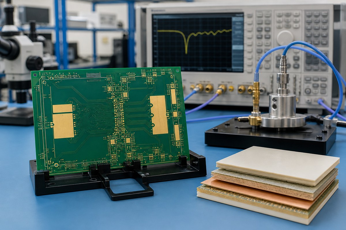
Material designation, Dk/Df source, glass construction and thermal requirements can affect the result. The customer identifies approved materials or measurable parameters and any alternatives.
EBest does not treat similar catalog values as automatic equivalence.
Impedance structures need complete identification
Target, tolerance, single-ended or differential type, layer, reference plane, mask condition and geometry restrictions are required. Critical net classes should map to these structures.
A global impedance note without layer information is returned for clarification.
Manufacturing geometry accounts for the real process
Etching and plating influence finished trace width and spacing. Our fabrication team may propose production geometry for the approved stack-up and impedance target.
The customer approves any change to released dimensions. Compensation is controlled, not applied as an invisible redesign.
Reference planes and dielectric relationships remain fixed
Controlled traces depend on their intended plane and dielectric. Plane openings, layer transitions and hybrid material regions can change the electrical environment.
Our review identifies manufacturing-data inconsistencies; the customer decides electrical acceptability.
Differential pairs require coupling assumptions
Pair impedance can be reached with different trace and spacing combinations. State whether individual impedance, pair spacing, intra-pair skew or another geometry is fixed.
The approved structure is represented in the coupon and manufacturing data.
Via structures depend on the final stack-up
Blind, buried, microvia and backdrill layer pairs must align with the released layer order and thickness. Drill, pad, anti-pad, fill, cap and remaining-stub requirements need explicit definitions.
A stack-up change triggers drill and backdrill review.
Coupons provide defined production evidence
Coupon structures, panel location, measurement method, target and tolerance are agreed before fabrication. The report connects results to the lot and structure.
A coupon does not prove every routed trace, via discontinuity or complete system channel.
Panel position and copper distribution can affect representation
Coupons and production boards share a panel but may not occupy identical locations or local copper environments. Where the customer has a special representation requirement, coupon position and surrounding construction are defined before panel release.
EBest records the agreed relationship and does not claim that one coupon measures every local variation.
Solder mask conditions belong in the impedance definition
Outer-layer traces may be covered, partially covered or exposed. Mask can affect the effective structure and the geometry used for a coupon. The customer identifies the modeled condition and any no-mask region.
Fabrication data and the coupon reproduce the approved state as closely as the agreed design permits.
Fabrication tolerance and design margin are different
EBest confirms the manufacturing tolerance proposed for the structure. The customer determines whether that tolerance fits the channel’s electrical margin and whether tighter controls or a different stack-up are needed.
This decision is made before production rather than after a coupon result approaches the limit.
Out-of-tolerance results receive controlled disposition
Affected lots are identified and reviewed. Investigation can include coupon identity, measurement setup, material, construction and process data.
Any concession follows the customer workflow, and original results remain in the record.
Stack-up and impedance control matrix
| Input | EBest control | Evidence by agreement |
|---|---|---|
| Layer order and function | Cross-file reconciliation | Released stack-up |
| Material and dielectric | Approved identity and construction | Applicable material/build record |
| Copper and geometry | Process-aware production proposal | Approved dimensions |
| Impedance target | Defined structure and coupon | Lot-linked measurement report |
| Via/backdrill | Layer-pair and depth control | Specified structural inspection |
Repeat orders protect the same electrical construction
Before another lot, EBest rechecks material availability, stack-up, copper, geometry, coupon and special drill programs. Proposed changes are reviewed before use.
A previous passing report does not approve a different material or layer build.
Inputs for an EBest stack-up review
- PCB data and fabrication drawing.
- Target layer order and finished thickness.
- Approved materials and copper by layer.
- Critical net classes and reference planes.
- Impedance targets, tolerances and mask state.
- Nominal geometry and fixed constraints.
- Via, microvia and backdrill requirements.
- Coupon, report and change-notification rules.
What EBest returns
Our PCB engineers can return a manufacturable stack-up proposal, unresolved material and geometry questions, impedance structure table, coupon plan, via review and available production evidence. Send the electrical assumptions with the construction so both teams approve the same board before fabrication.
Discuss Your Project With Our Engineers
Send us your stack-up, impedance table, layer references, material restrictions and finished-thickness requirement. We will return a manufacturable construction and coupon plan for approval.
Email sales@ebestpcba.com with the current revision and expected quantity.
For your controlled-impedance board, we will confirm the stack-up, trace geometry, coupon and report requirement before fabrication. You can approve the construction against the target for each named layer and structure.