Introduction
The TL072 pinout consists of 8 pins supporting 2 independent operational amplifiers, with separate inputs and outputs and shared positive and negative power supplies. Each amplifier has an inverting input, a non-inverting input, and an output. Understanding these connections is essential when designing audio amplifiers, active filters, sensor interfaces, and other analog circuits. This guide covers the TL072 pinout diagram, datasheet specifications, DIP/SMD packages, wiring diagrams, amplifier circuits, and equivalent ICs.
At EBest PCBA, we provide PCB fabrication, electronic component sourcing, SMT/DIP assembly, and functional testing for analog and mixed-signal products. Our services include Free DFM, No MOQ, 4 SMT production lines, and MES single-board traceability, with 1 sales representative and 3 engineers supporting the project. Send Gerber files, BOM, quantities, and testing requirements to sales@ebestpcba.com for an engineering review and quotation.
Key Takeaways
- The TL072 is a dual operational amplifier with 2 independent amplifier channels in a single IC, used in audio circuits, active filters, and analog signal conditioning.
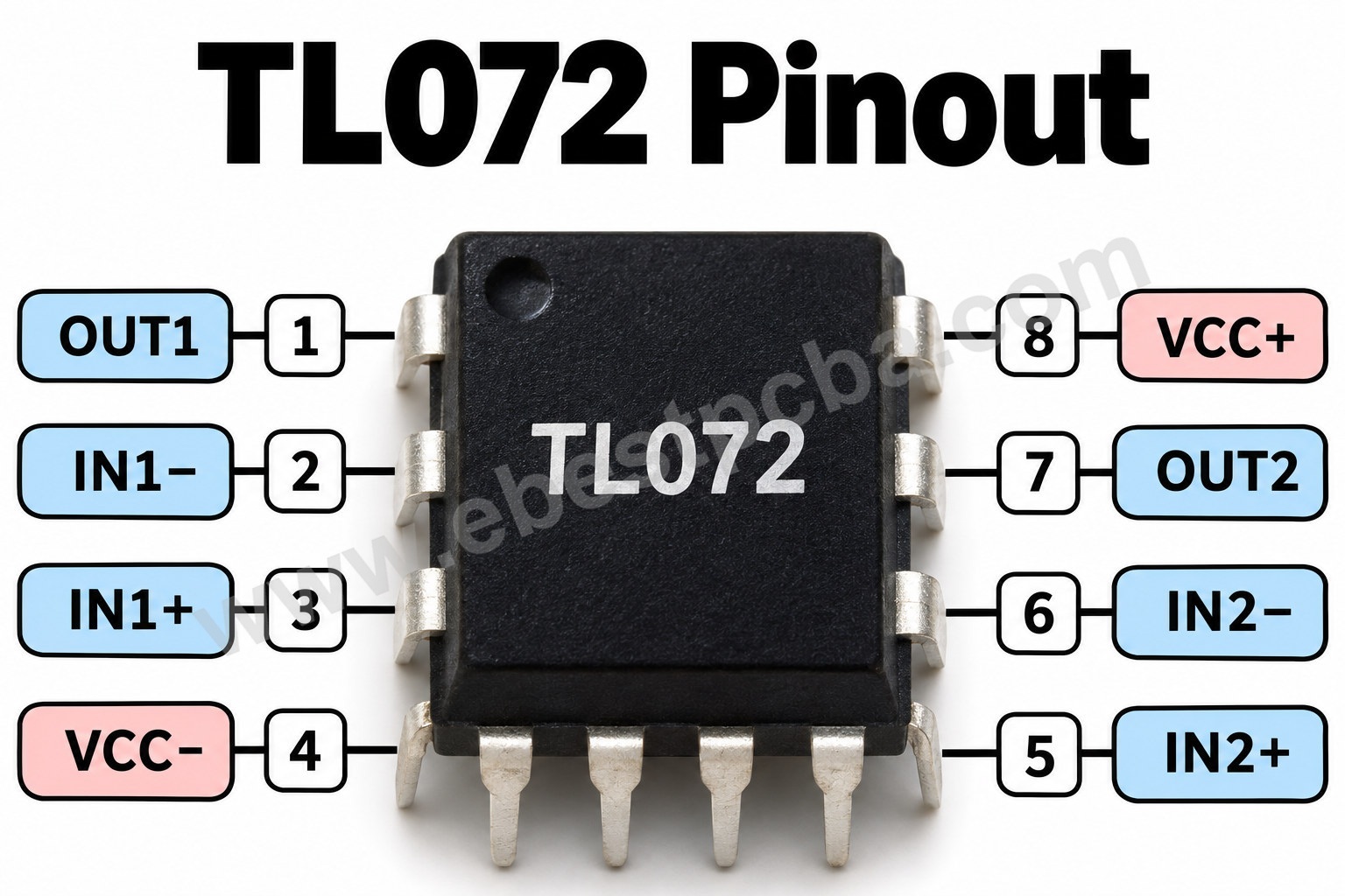
- The standard TL072 pinout has 8 pins: Pins 1–3 control amplifier 1, Pins 5–7 control amplifier 2, Pin 4 is VCC−, and Pin 8 is VCC+.
- TL072 DIP-8 and SMD versions share the same functional pin arrangement in corresponding standard 8-pin packages, but have different PCB footprints.
- The classic TI TL072 supports a total supply range of 7–30 V, with a typical 3 MHz gain-bandwidth product and 13 V/µs slew rate.
- TL072 circuits can be configured as non-inverting amplifiers, inverting amplifiers, or voltage followers using appropriate feedback networks.
- TL082, LF353, NE5532, LM358, and RC4558 are replacement candidates, but matching pin functions do not guarantee electrical interchangeability.
- TL072 PCB design requires power decoupling, correct Pin 1 orientation, short feedback paths, and careful high-impedance input routing.
- EBest PCBA supports TL072 PCB manufacturing and assembly through component sourcing, Free DFM, SMT/DIP assembly, testing, and No MOQ services.
What Is the TL072 Pinout and Pin Configuration?
The TL072 is an 8-pin dual operational amplifier containing 2 channels that share supply connections. Amplifier 1 uses Pins 1, 2, and 3; amplifier 2 uses Pins 5, 6, and 7. Pin 4 is the negative supply terminal, and Pin 8 is the positive supply terminal.
| Pin | Pin Name | Function |
|---|---|---|
| 1 | OUT1 | Amplifier 1 output |
| 2 | IN1− | Amplifier 1 inverting input |
| 3 | IN1+ | Amplifier 1 non-inverting input |
| 4 | VCC− | Negative supply |
| 5 | IN2+ | Amplifier 2 non-inverting input |
| 6 | IN2− | Amplifier 2 inverting input |
| 7 | OUT2 | Amplifier 2 output |
| 8 | VCC+ | Positive supply |
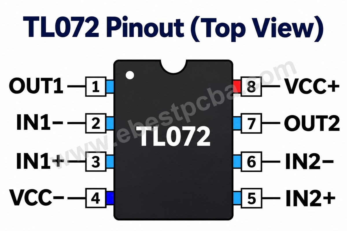
The package notch or Pin 1 marker defines orientation; numbering proceeds counterclockwise in the top view.
Amplifier 1 (Pins 1–3): Pin 1 is its output; Pin 2 is its inverting input, usually connected to negative feedback; Pin 3 is the non-inverting input.
Amplifier 2 (Pins 5–7): Pin 5 is its non-inverting input; Pin 6 is its inverting input; Pin 7 is its output.
Power pins (4 and 8): Pin 4 connects to VCC− and Pin 8 to VCC+. In a ±12 V circuit, Pin 4 connects to −12 V, Pin 8 to +12 V, and signal ground is 0 V. In a suitable single-supply circuit, VCC− may be grounded, but input and output range limits still apply.
What Are the Key Specifications in the TL072 Datasheet?
The TL072 is a dual FET-input operational amplifier. For the classic Texas Instruments TL072, the typical gain-bandwidth product is 3 MHz, the typical slew rate is 13 V/µs, and the total supply range is 7–30 V. Values depend on the exact device, temperature, load, and datasheet test conditions.
| Parameter | Classic TI TL072 specification |
|---|---|
| Amplifier channels | 2 |
| Input architecture | FET input |
| Total supply voltage | 7–30 V |
| Gain-bandwidth product | 3 MHz typical |
| Slew rate | 13 V/µs typical |
| Input voltage noise | 37 nV/√Hz typical at 1 kHz |
| Common-mode rejection | 100 dB typical |
| Package choices | Manufacturer/orderable-part dependent |
FET input stage: Low input bias current helps when buffering relatively high-impedance sources in analog measurement and audio applications. Input offset voltage, input leakage, board contamination, and noise remain important.
Gain-bandwidth product: A simplified relationship for a dominant-pole amplifier:
» Bandwidth ≈ GBW / closed-loop noise gain
A noise gain of 10 implies an approximate 300 kHz bandwidth with a 3 MHz GBW; real performance varies by topology and loading.
Slew rate: For a sinusoidal output, the approximate minimum required slew rate:
» SR ≥ 2π × frequency × Vpeak
A 20 kHz, 5 V-peak output requires about 0.628 V/µs, below the classic TL072’s typical 13 V/µs specification. Designers still need to verify distortion, signal swing, bandwidth, and loading.
Power range: The classic TL072 is not rail-to-rail. It needs appropriate headroom between its inputs/outputs and the supply rails, especially in single-supply applications.
TL072H is different: The newer TL072H has updated performance, including a typical 5 MHz GBW and 20 V/µs slew rate. Never apply TL072H figures to a classic TL072 without checking the exact part.
Official reference: Texas Instruments TL072 datasheet.
Is the TL072 SMD Pinout the Same as the DIP-8 Version?
Yes. Corresponding standard 8-pin TL072 SMD and DIP versions share functional pin assignments. Their physical package geometry, lead pitch, and PCB land patterns are different.
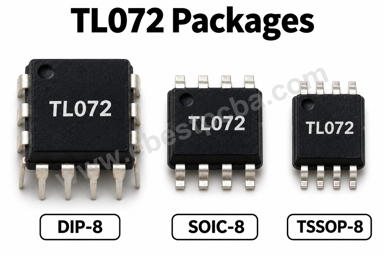
| Package | Assembly | Design consideration |
|---|---|---|
| PDIP-8 | Through-hole | Drilled pads and wider lead spacing |
| SOIC-8 | SMT | Gull-wing footprint and reflow assembly |
| TSSOP-8 | SMT | Smaller body and finer lead pitch |
| SOP-8 | SMT | Verify exact manufacturer drawing |
DIP-8: The top view shows 4 leads on each side with the notch marking the top. It is practical for socketed prototypes and through-hole circuits.
SOIC-8: It retains the same pin functions, but uses gull-wing surface-mount leads and an SOIC land pattern.
TSSOP-8: It retains the usual 8-pin functional assignment but requires a smaller and finer-pitch footprint.
TL072CP, TL072CN, and TL072IP: Suffixes are manufacturer-specific. TI TL072CP, for example, is a PDIP-8 orderable part. Confirm the complete manufacturer part number, package drawing, and grade before sourcing or approving substitutions. DIP and SMD packages cannot share one physical PCB footprint without an adapter or board change.
How to Connect the TL072 Pinout in a Circuit Diagram?
To wire a TL072, connect Pin 8 to VCC+ and Pin 4 to VCC−, then connect the amplifier signal pins according to the chosen circuit and apply a suitable negative-feedback network. A ±12 V dual supply is a convenient example.
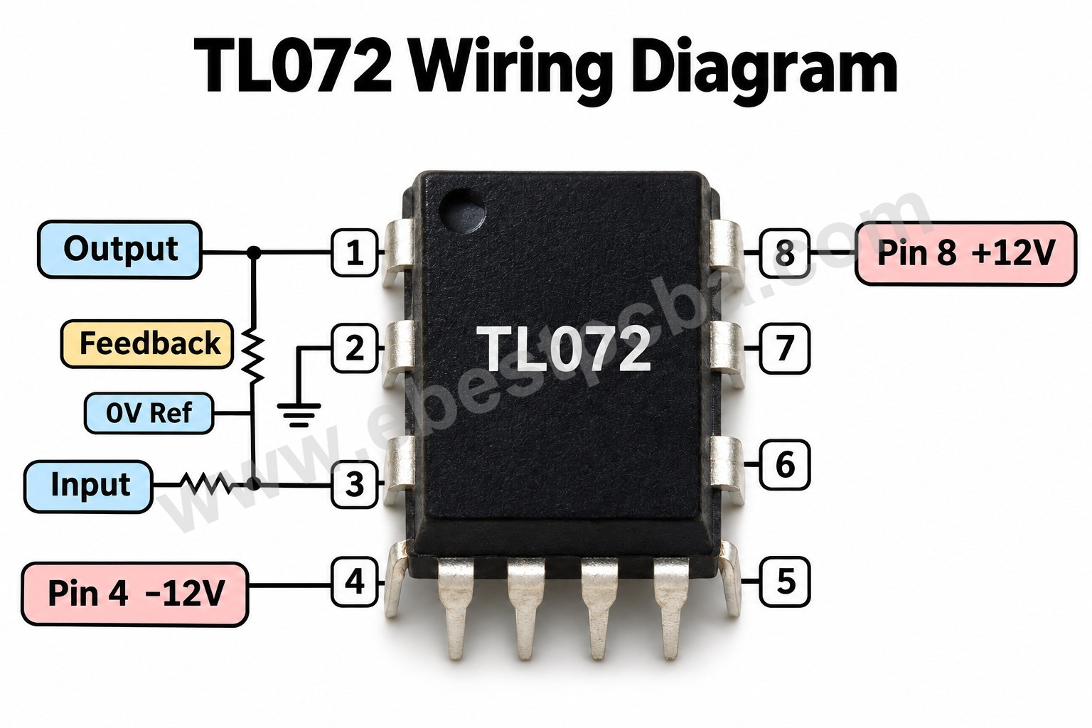
Diagram note: The accompanying generated wiring illustration is a conceptual visual only. Its feedback connections are not a verified buildable schematic. For wiring, follow the pin table and the explicit connections below, and verify the final circuit against the manufacturer’s datasheet.
| Connection | TL072 pin | Dual-supply example |
|---|---|---|
| Positive supply | 8 | +12 V |
| Negative supply | 4 | −12 V |
| Amplifier 1 output | 1 | Output / feedback node |
| Amplifier 1 inverting input | 2 | Feedback network |
| Amplifier 1 non-inverting input | 3 | Signal input |
| Signal reference | External 0 V node | Ground reference |
Feedback wiring example: For amplifier 1 in a non-inverting stage, take the signal into Pin 3, connect Rf between Pin 1 and Pin 2, and connect Rg between Pin 2 and the 0 V signal reference. The output is on Pin 1. The second amplifier has its own inputs (5 and 6) and output (7).
Decoupling: Place suitable bypass capacitors, often starting with 100 nF ceramic capacitors, close to the IC supply pins, with short return connections to the appropriate reference plane. Check the actual power-distribution network before finalizing capacitor connections.
Single supply: With a suitable single supply, Pin 4 may connect to ground and Pin 8 to the positive rail. An AC signal may need a buffered mid-supply bias point, and its input and output swing must satisfy the classic TL072’s non-rail-to-rail limitations.
How to Build a TL072 Amplifier Circuit?
The TL072 supports non-inverting, inverting, and unity-gain buffer configurations. Feedback resistors determine gain; the power rails, amplifier input common-mode range, and load requirements determine feasible operating levels.
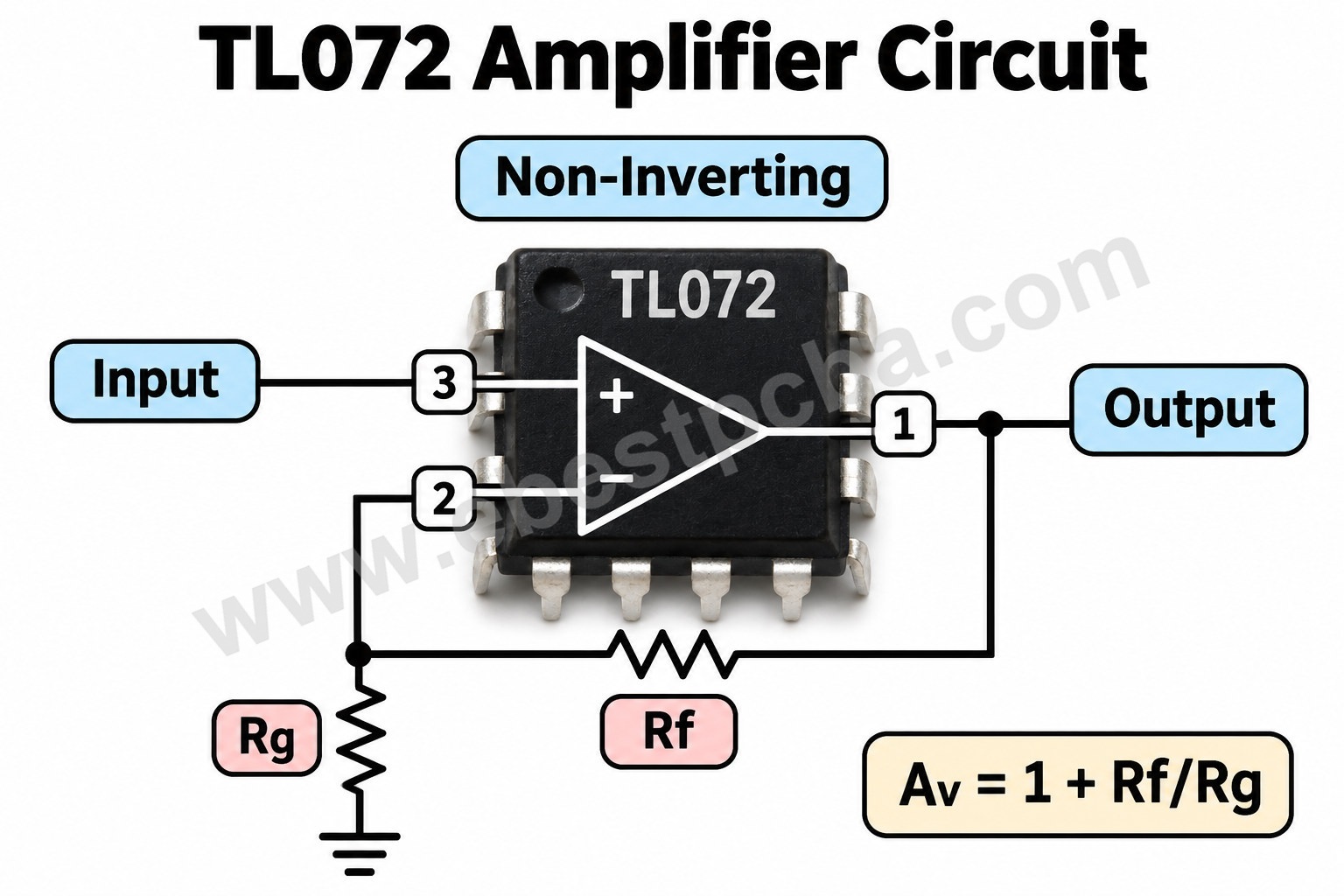
1. Non-Inverting Amplifier
- Signal input to Pin 3 (IN1+).
- Feedback resistor Rf from Pin 1 (OUT1) to Pin 2 (IN1−).
- Resistor Rg from Pin 2 to the signal reference.
- Output from Pin 1.
Ideal voltage gain:
» Av = 1 + Rf / Rg
With Rf = 20 kΩ and Rg = 10 kΩ, ideal closed-loop gain is Av = 3. A 0.5 V-peak signal ideally produces about 1.5 V peak while the circuit stays in its linear range.
2. Unity-Gain Buffer
Use the second amplifier by connecting the input to Pin 5, the output at Pin 7, and Pin 7 back to Pin 6. Ideal gain is 1. This provides buffering for compatible high-impedance sensors or audio signals.
3. Inverting Amplifier
Connect the input through Rin to Pin 2 and Rf from Pin 1 to Pin 2. Tie Pin 3 to the appropriate signal reference.
» Av = −Rf / Rin
With 100 kΩ and 10 kΩ, ideal gain is −10.
| Circuit | Ideal voltage gain | Use |
|---|---|---|
| Non-inverting | 1 + Rf / Rg | Signal amplification |
| Inverting | −Rf / Rin | Inverted gain |
| Follower | 1 | Buffering |
Real circuits must be checked for bandwidth, stability, common-mode range, output swing, and load. For build-ready drawings, use a verified schematic and component datasheets.
What Are the Best TL072 Equivalent Op Amps?
TL072 equivalent IC selection requires more than matching the pin numbers: verify the exact device, supply range, input limits, stability and load requirements.
TL072H, TL082, LF353, NE5532, LM358, and RC4558 may be considered in place of TL072 in selected applications. Corresponding standard 8-pin dual-op-amp versions can share functional pinouts, but they may differ significantly in input architecture, noise, bias current, speed, voltage limits, and output range.
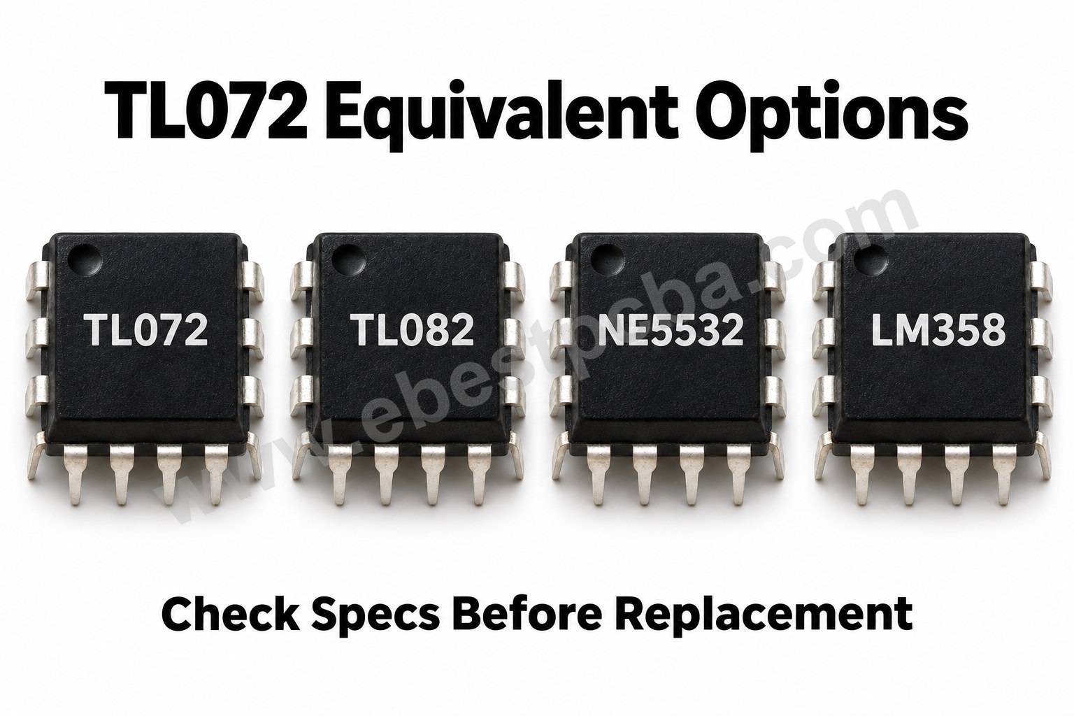
| Candidate | Standard 8-pin functional pinout | Selection check |
|---|---|---|
| TL072H | Common dual-op-amp mapping | Revised voltage and performance |
| TL082 | Common dual-op-amp mapping | Noise, bias, and offset |
| LF353 | Common dual-op-amp mapping | Supply and input characteristics |
| NE5532 | Common dual-op-amp mapping | Bipolar input bias and noise |
| LM358 | Common dual-op-amp mapping | Speed and input/output range |
| RC4558 | Common dual-op-amp mapping | Bias, noise, and headroom |
TL072H: An upgraded version with different electrical performance; compare exact orderable parts and operating limits.
TL082: A FET-input dual op amp often considered for general analog designs; compare offset and noise requirements.
LF353: Another JFET-input dual amplifier; compare operating voltage and availability.
NE5532: Often used in low-noise audio circuits, but its bipolar input bias current can create offset across high source resistance.
LM358: Common in low-frequency sensing and control; classic versions generally have lower bandwidth/slew rate than TL072 and different input/output voltage limits.
RC4558: Seen in audio and older analog designs; review its noise, bias, bandwidth, and supply requirements.
Do not approve replacement solely because an IC fits the same socket or has the same pin numbering.
TL072 vs LM358 vs NE5532 vs 4558: Are Their Pinouts Compatible?
Yes, their corresponding standard 8-pin dual-amplifier packages can have the same functional pin map. However, electrical performance and package-specific requirements must be evaluated before substitution.
| Pin | TL072 | LM358 | NE5532 | RC4558 |
|---|---|---|---|---|
| 1 | OUT1 | OUT1 | OUT1 | OUT1 |
| 2 | IN1− | IN1− | IN1− | IN1− |
| 3 | IN1+ | IN1+ | IN1+ | IN1+ |
| 4 | V− | V− | V− | V− |
| 5 | IN2+ | IN2+ | IN2+ | IN2+ |
| 6 | IN2− | IN2− | IN2− | IN2− |
| 7 | OUT2 | OUT2 | OUT2 | OUT2 |
| 8 | V+ | V+ | V+ | V+ |
Input architecture: TL072 uses FET inputs; classic LM358, NE5532, and RC4558 use bipolar input stages. Different bias currents affect high-impedance sources. As an illustration, a 200 nA bias current through 100 kΩ develops Verror = Ib × R = 20 mV; this is not a specification for any particular candidate.
Speed and noise: The classic TL072’s typical GBW is 3 MHz and slew rate is 13 V/µs. Other op amps differ, so compare performance at the intended closed-loop gain and output amplitude.
Voltage and output swing: The same socket does not imply the same minimum supply voltage, input common-mode range, or output headroom. Verify the actual rails and load conditions.
Application-specific decision: Prioritize leakage and bias current for sensor buffers, noise and distortion for audio, and voltage/headroom and stability for low-voltage control. Confirm performance through measurements before production substitution.
What PCB Design and Assembly Issues Should You Check for TL072?
TL072 PCB design should focus on correct package footprint and Pin 1 orientation, local power decoupling, compact feedback routing, and clean high-impedance input paths. Errors in these areas may cause noise, unexpected gain, oscillation, or assembly faults.
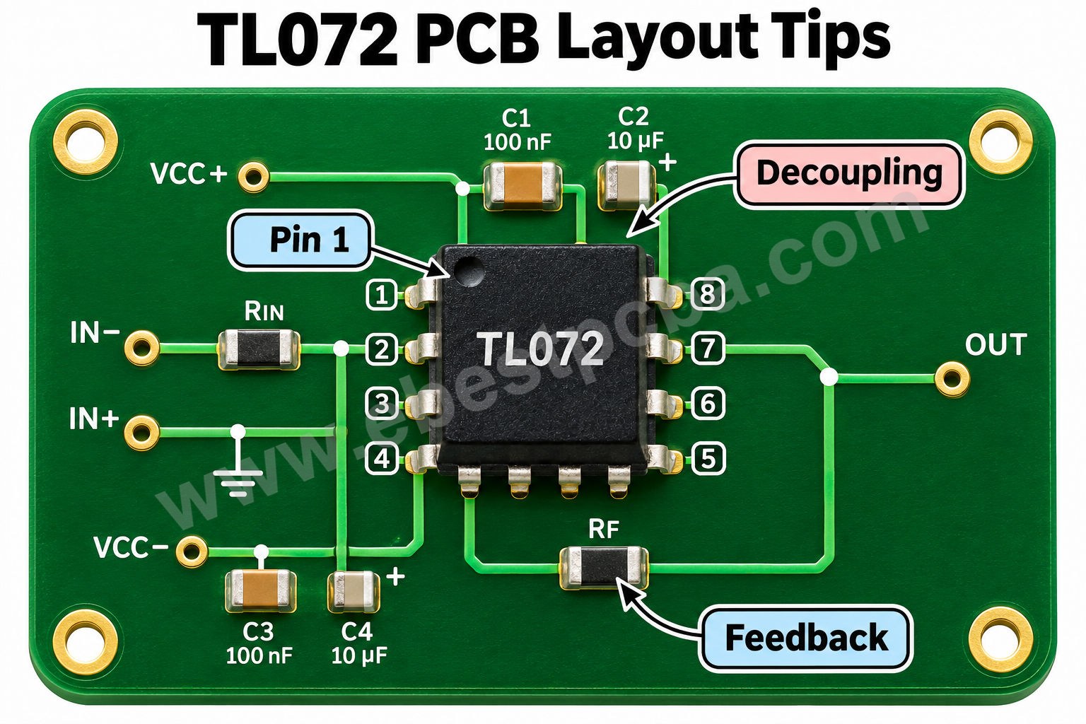
Layout illustration note: The AI-generated board image is a visual aid, not an electrically verified PCB layout. In particular, amplifier 1 uses Pin 1 as its output, while Pin 7 belongs to amplifier 2. Use the netlist, approved schematic, and datasheet for actual design and manufacturing.
- Footprint and Pin 1: Confirm the complete manufacturer part number, body/lead geometry, pin numbering, and pad shape before releasing Gerbers.
- Supply decoupling: Place suitable ceramic bypass capacitors close to Pins 4 and 8 and provide appropriate return paths.
- Feedback loop: Keep the feedback network near the amplifier’s output and inverting input to reduce parasitics.
- Input routing: Keep sensitive high-impedance paths away from switching nodes and noisy high-current traces. Consider leakage, humidity, contamination, and guarding for precision applications.
- Unused amplifier: Use a stable defined configuration, for example a unity-gain buffer biased at an allowed input voltage, rather than leaving inputs floating.
- Assembly checks: Verify component orientation, feedback resistor values, solder joints, BOM and assembly drawing consistency.
| Symptom | Possible cause | First check |
|---|---|---|
| No output | Power or soldering fault | VCC+/VCC− and connections |
| Saturated output | Common-mode or feedback issue | Input levels and feedback |
| Oscillation | Layout or capacitive load | Feedback and decoupling |
| Excess noise | Supply or coupling | Ground/reference routing |
| Wrong gain | Incorrect resistors | BOM and resistor values |
| Intermittent fault | Poor solder joint | Visual/electrical inspection |
EBest PCBA can review footprint compatibility, Pin 1 marking, BOM clarity, and assembly constraints as part of its DFM process. AOI and customer-defined electrical/functional tests can help verify the finished board.
Why Choose EBest PCBA for TL072 PCB Assembly?
EBest PCBA combines component sourcing, PCB fabrication, SMT/DIP assembly, inspection, and functional testing for TL072 analog amplifier PCBs and mixed-signal products. Its coordinated manufacturing services help customers move from validated designs to prototype builds and repeat orders.
- Free DFM Review: Feedback on footprint, Pin 1 orientation, pad dimensions, component clearance, and assembly risks.
- No MOQ: Prototype and small-batch support without a fixed minimum order quantity.
- 4 SMT Production Lines: 2 JUKI and 2 YAMAHA lines for automated assembly.
- SMT and Through-Hole Assembly: Suitable processes for TL072 SMD and DIP-style packages and mixed-technology PCBs.
- Component Sourcing: BOM-based purchasing and discussion of approved alternate parts.
- Inspection and Testing: SPI, AOI, X-Ray, ICT, and FCT capabilities as applicable to the assembly and test plan.
- MES Traceability: Single-board production record retrieval.
- Engineering Support: 1 sales representative + 3 engineers coordinate design review and production questions.
Applicable quality-system certifications include ISO 9001, ISO 13485, IATF 16949, and AS9100D, subject to supplier qualification and relevant certification scopes.
For a TL072 amplifier PCB, audio circuit board, sensor interface, or full PCBA project, send Gerber files, BOM, pick-and-place data, quantities, and test requirements to sales@ebestpcba.com for project-specific review and quotation.
Frequently Asked Questions About TL072 Pinout
1. Is TL072 a dual or single operational amplifier?
TL072 contains 2 independent amplifiers sharing positive and negative supply pins. Each has an inverting input, a non-inverting input, and an output. The amplifiers may operate separately or be connected in a multistage analog circuit.
2. What is the difference between TL071, TL072, and TL074?
TL071 is a single amplifier, TL072 is dual, and TL074 is quad. Their package pinouts differ according to channel count; standard TL074 versions typically use 14 pins rather than the TL072’s 8.
3. Can TL072 operate with a single power supply?
Yes, when total supply voltage and signal ranges meet the device’s specification. A mid-supply reference may be needed for AC signals; the classic TL072 is not rail-to-rail, so check its input common-mode range and output headroom.
4. Are TL072CP and TL072CN pin-compatible?
Corresponding 8-pin DIP variants commonly use the standard TL072 functional assignments, but suffixes are manufacturer-specific. Check the exact part number, package, temperature grade, and datasheet before approving a substitute.
5. Can TL082 replace TL072 without changing the PCB?
In matching standard 8-pin versions, TL082 may share the TL072 pin arrangement. Verify noise, offset, bias, supply range, bandwidth, and the operating circuit before deciding that it is electrically suitable.
6. What happens if TL072 Pin 4 and Pin 8 are reversed?
Reverse power connections can damage the IC. Pin 8 is the positive supply and Pin 4 is the negative supply. Verify orientation and rail polarity before powering the board.
7. What should I do with the unused TL072 amplifier?
Configure the unused amplifier in a stable defined state. A common approach is to connect its output to its inverting input and bias the non-inverting input at a voltage permitted by the selected power rails and input common-mode range.
Conclusion
The TL072 pinout provides 2 independent amplifier channels with shared supply pins in a standard 8-pin configuration. Correct pin identification, stable power, matching footprints, and appropriate feedback are important in audio, filtering, and signal-buffer applications. Equivalent parts must be evaluated for electrical performance as well as pin compatibility. EBest PCBA supports TL072 projects with Free DFM, component sourcing, No MOQ, SMT/DIP assembly, testing, and MES traceability. Send your design data and BOM to sales@ebestpcba.com for a tailored manufacturing quotation.
Technical references: Texas Instruments TL07x datasheet · TL072 product overview. AI-generated electrical illustrations are illustrative and not production-approved schematics.