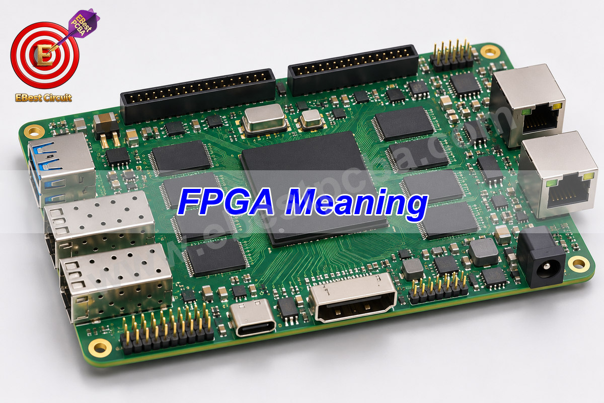
FPGA stands for field-programmable gate array. You configure this chip to build a digital circuit. A camera board might use one circuit to take in pixels, another to filter them and a third to send them out. Those circuits can work on different pixels at the same time.
Key Takeaways
- An FPGA is a configurable chip. The PCB carries the chip and connects it to other parts.
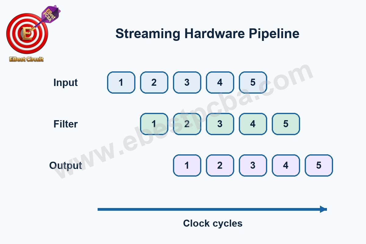
- A hardware pipeline can accept a new sample before the previous sample reaches the output.
- Check the clocks, constraints and startup sequence before testing the full design.
What Does FPGA Stand For in Electronics?
Field-programmable means you can configure the device after it leaves the factory. Gate array refers to the logic resources you connect to build the circuit. The logic may count pulses, move data between interfaces or perform arithmetic on a stream of samples.
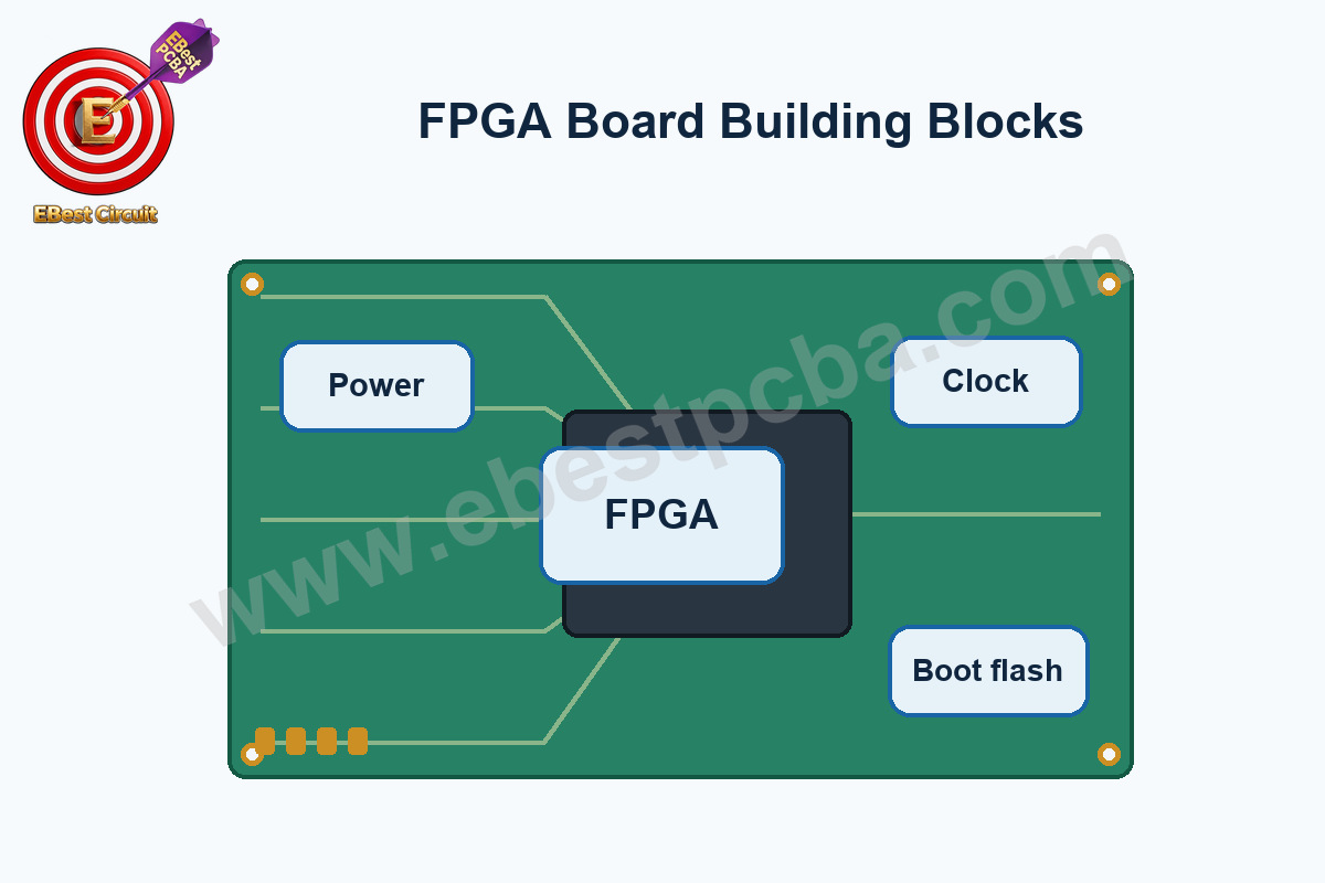
The FPGA is the chip. The PCB is the board that carries it. An FPGA board also needs supporting parts such as regulators, clocks, connectors and a way to load its configuration. A development kit often has extra ports for experiments. A production board only needs the parts for the job.
How Does FPGA Architecture Implement a Circuit?
FPGA architecture gives you small logic functions, registers and routes that connect them. A lookup table maps input bits to an output. A flip-flop holds a bit until a clock edge. Depending on the device, you can also use memory blocks, dedicated arithmetic and high-speed I/O.
| Resource | Typical job |
|---|---|
| LUT and flip-flop | Decode signals or store a pipeline stage |
| Programmable routing | Connect logic, memories and I/O |
| Block RAM | Buffer samples, packets or image lines |
| DSP block | Multiply and accumulate signal samples |
| I/O or transceiver block | Connect to external devices at supported rates |
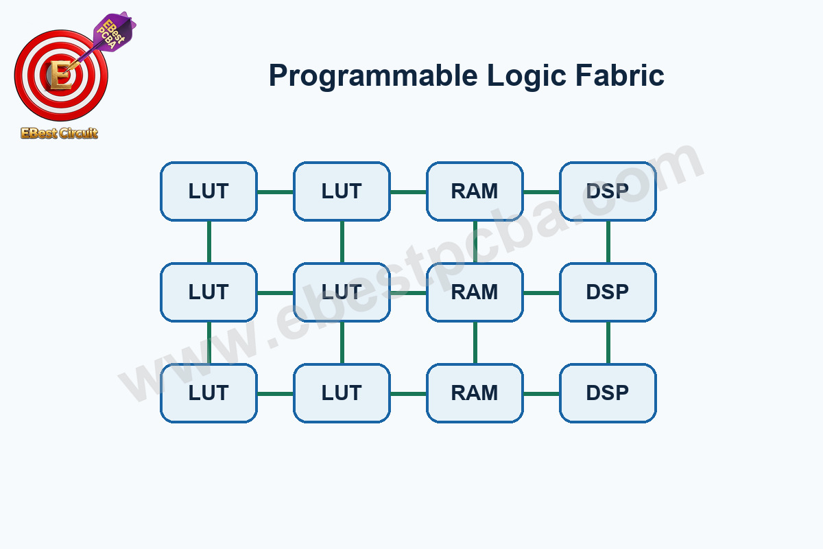
For a camera filter, memory holds a line of pixels while the arithmetic uses neighboring samples. A register passes each result to the next stage on a clock edge. That division lets several samples be in flight together.
How Does a Pipeline Improve Throughput Without Eliminating Latency?
Take a filter with four registered stages at 100 MHz. One clock cycle lasts 10 ns. If the filter accepts a sample every cycle, it can accept 100 million samples per second once it is running. A particular sample still takes about 40 ns to cross the four stages in this example.
The whole board may take longer. A converter needs time to produce the samples, a buffer can fill and the output link may pause. To check sustained throughput, run a long stream and let the receiver stall. Confirm that no samples are lost when the buffer fills.
| Quantity | What it measures | Example assumption |
|---|---|---|
| Clock period | Time between active edges | 10 ns at 100 MHz |
| Initiation interval | Cycles between accepted samples | One cycle with no stalls |
| Pipeline latency | Cycles from input acceptance to output | Four cycles in this example |
| Sustained throughput | Samples delivered over time | Limited by the slowest stage or interface |
Use the 100 MHz calculation to separate throughput from delay. The routed design and the actual interfaces determine whether the hardware can run at that rate.
How Does FPGA Programming Differ From Software?
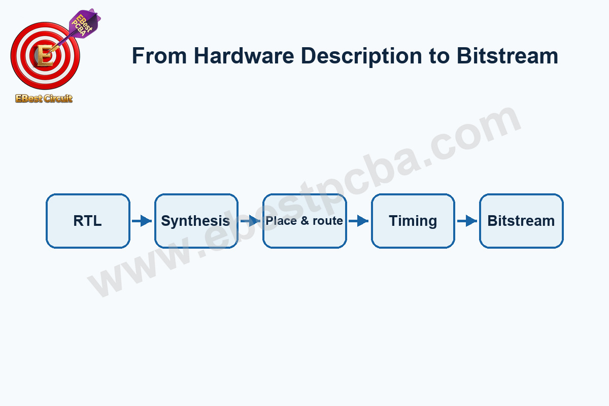
FPGA programming starts with a description of the hardware. You can write it in Verilog, SystemVerilog or VHDL, or connect existing blocks. Simulate the logic, then let the tools synthesize, place and route it. Check timing before loading the resulting bitstream.
After the bitstream loads, check startup and reset on the board. Confirm that pin assignments and I/O voltages match the schematic. Many SRAM-based parts load their configuration at each power-up. Check the startup method for the part on the BOM.
What Does a Timing Report Tell You Before You Load the FPGA?
Before reading the slack numbers, check the constraints. List the clocks and external interfaces that the design actually uses. A timing report only checks paths that have the applicable constraints.
At 100 MHz, the clock period is 10 ns. The receiving register needs the data to arrive before its setup window, and the sending register takes time to produce it. That leaves less than 10 ns for the logic and routing. If a path is late, moving a register boundary can shorten it. Check hold timing separately.
For a signal crossing between unrelated clocks, decide what has to cross. A single control level can use a synchronizer. A short pulse may need a handshake or stretching. A stream of data may need an asynchronous FIFO so the receiver gets complete samples in order.
When Does an FPGA vs Microcontroller Comparison Matter?
An FPGA vs microcontroller comparison starts with a timing requirement. For a temperature reading every second, a microcontroller and its peripherals may be enough. For several data lanes that must be sampled together and processed as they arrive, an FPGA can build a separate path for each lane. Check whether timers, DMA or a dedicated peripheral already meet the requirement before adding another device.
| Requirement | Usually start with |
|---|---|
| Periodic sensor reads and user interface | Microcontroller |
| Several synchronized channels with custom timing | FPGA |
| Fixed algorithm at high volume after requirements settle | Evaluate an ASIC against FPGA and MCU |
| Control software plus custom real-time interfaces | FPGA plus processor, or an FPGA SoC |
What Should You Check Before Building an FPGA PCB?
Start at the schematic with the power rails, clocks and configuration pins. Confirm that each I/O bank can use the voltage of the devices connected to it. If a BGA needs inner-row escape routing, check that the board stackup and assembly plan support the chosen package.
Send the part number, pin constraints and startup sequence with the PCB design review. Include the approved bitstream and its expected status indications when requesting PCBA assembly service and inspection and testing.
How Do You Bring Up an FPGA Board That Will Not Configure?
If the board never finishes configuration, start with power, reset and boot mode. Once configuration finishes, use a small test image to check the clock and a known output before bringing up memory or high-speed links.
- Confirm the rail voltages, current draw and power-good sequence against the selected family’s documentation. Measure at the load rather than only at the supply connector.
- Check the reference clock and reset signal. Verify the strap settings for the intended boot mode and that the configuration interface operates at the correct voltage.
- Confirm the bitstream matches the exact device and boot settings. Read the device-specific configuration status through the supported interface.
- Load a known minimal test design that exercises a clock, one output and, if applicable, the board’s diagnostic connection. Then enable memory and high-speed interfaces in stages.
- Archive the tested bitstream version, tool version, board revision and results. A replacement board should be tested with the matching image and test procedure.
| Observation | Check first |
|---|---|
| Configuration status never completes | Rails, reset, mode straps and storage interface |
| Configuration completes but outputs are idle | Clock enable, reset release, pin map and I/O voltage |
| Works at room temperature only | Timing margin, rail droop and clock quality |
| Intermittent data errors | Crossing logic, interface timing and signal integrity |
Frequently Asked Questions
What is the difference between an FPGA and a PCB?
An FPGA is an integrated circuit you can configure. A PCB is the board with copper connections and pads that supports the FPGA, power supplies and other parts. You load a configuration into the FPGA. The PCB layout determines how the chip is connected.
Is an FPGA better than a CPU?
Choose for the workload. A CPU is a good fit for general-purpose software and changing control tasks. An FPGA is useful when several digital signals need to be handled in parallel with predictable timing. Compare the required latency and sustained data rate.
Can I reprogram an FPGA after installation?
Many devices support reconfiguration if the board provides the right interface. Check how the product loads a new image, whether it must stop during the update, and how it recovers if the update is interrupted.
What is the difference between a bitstream and firmware?
A bitstream configures logic and routing in the FPGA. Firmware is code a processor runs. A product with an FPGA and a processor can require both files.
Why can an FPGA run out of LUTs while memory is still free?
Logic tables and memory blocks are separate resources. Check how much of each the design uses and whether the place-and-route tools can meet timing at that utilization.
What should I include in the programming package for production?
Include the board revision, exact FPGA, approved bitstream and version, programming method and expected startup status. Give the test team an output or interface to check after loading the image.