Introduction
A dual inline package, usually abbreviated DIP or DIL, is an electronic component package with a rectangular body and two parallel rows of leads. In the common through-hole form, the leads enter holes in a PCB and are soldered, or plug into a matching socket. The package describes the physical connection format; it does not tell you what the circuit inside does.
For a PCB build, three checks prevent many avoidable errors: identify the correct pin-numbering view, match the exact package drawing to the footprint, and decide whether the component will be soldered directly or socketed. At EBest PCBA, we review those manufacturing inputs alongside your BOM and assembly drawings before confirming the build scope.
Key Takeaways
- DIP identifies a package format, rather than a particular IC function or electrical pin assignment.
- Conventional DIP pin numbering runs counterclockwise when viewed from the top; verify the device drawing and Pin 1 indicator.
- Lead pitch, row spacing and molded body width are different dimensions.
- A socket must match the package geometry and the application’s contact and mechanical requirements.
- Through-hole soldering, inspection and functional testing need a defined project scope.
Dual Inline Package Meaning
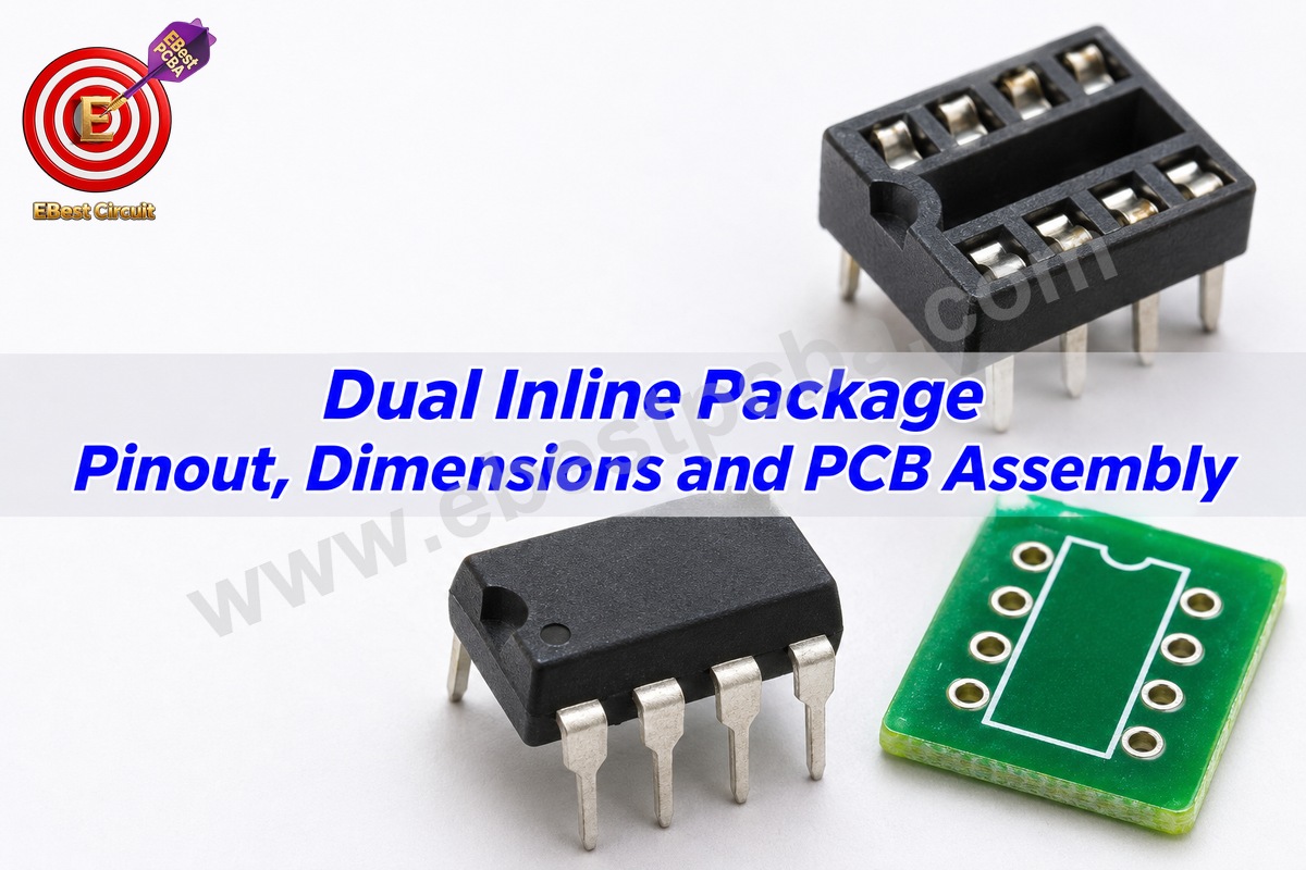
Dual inline package meaning refers to the component’s two rows of electrical leads. The term is commonly associated with ICs, but a similar package arrangement can also hold other component types. DIP-8, for example, identifies eight lead positions; it does not identify the IC as an amplifier, timer or memory device.
Manufacturers may write the name as dual in-line package, DIP or DIL. Plastic versions are often called PDIP, while ceramic versions may be called CDIP or CERDIP. Those labels help identify the family, but the complete manufacturer part number and package code remain the basis for purchasing and footprint selection. Texas Instruments’ package overview distinguishes plastic and ceramic DIP bodies and describes soldered and socketed use.
Do not confuse DIP with DIMM, a dual inline memory module. A DIMM is a module with edge contacts, rather than a conventional two-row through-hole IC package. A DIP switch is also a separate component function: its individual switch positions establish circuit settings.
How Do You Read DIP Pin Numbers?
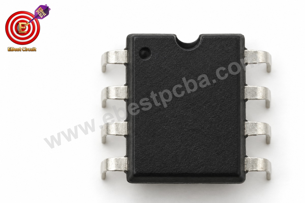
Read conventional DIP numbering from the package’s top view, locate Pin 1, and follow the numbers counterclockwise. The notch or index mark establishes orientation; the datasheet confirms which mark to use. A molded circle elsewhere on the body should not automatically be treated as the Pin 1 indicator.
With an eight-pin package’s notch at the top, Pins 1–4 descend along the left side. Pin 5 is at the lower right, and Pins 6–8 continue upward. A bottom view mirrors that arrangement. Keep the view explicit when checking an assembly drawing or PCB library.
| Position, notch at top | 8-pin DIP number |
|---|---|
| Left side, top to bottom | 1, 2, 3, 4 |
| Right side, top to bottom | 8, 7, 6, 5 |
These are physical pin numbers, not signal names. Two DIP-8 ICs can assign different functions to the same numbered pin. Our TL072 pinout guide shows why the device-specific pin table must accompany the package outline. Never infer supply polarity or output connections from the package shape alone.
Dual Inline Package Dimensions
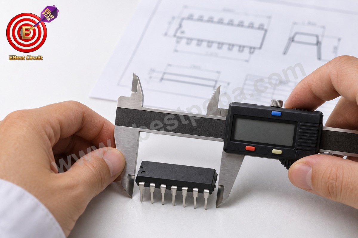
Dual inline package dimensions must come from the exact manufacturer’s package drawing. Matching the pin count alone is insufficient: adjacent-lead pitch, distance between rows, body size and lead cross-section all affect whether the part fits.
A 2.54 mm lead pitch is common in conventional DIP packages, but it is not a universal rule for every dual-row format. A narrow package may use a nominal 7.62 mm row arrangement; the molded body width is a separate measurement. For example, a component-specific Power Integrations package drawing distinguishes the 2.54 mm pitch, body dimensions and lead-row geometry. That example is not a generic footprint for every eight-pin device.
| Dimension | What it describes |
|---|---|
| Lead pitch | Center-to-center spacing of adjacent leads in one row |
| Row spacing | Separation of the two lead rows at the specified drawing reference |
| Body length and width | Molded package outline and occupied space |
| Lead width and thickness | Rectangular lead cross-section relevant to hole clearance |
| Body height and lead length | Vertical clearance, insertion depth and underside protrusion |
Separate maximum dimensions from nominal or basic values, and check how the drawing defines the seating plane. Do not select a drill diameter by copying lead pitch. A rectangular lead must pass through the finished plated hole with suitable clearance; the PCB fabricator also needs to distinguish finished-hole requirements from production drill sizes.
A practical release check is to compare the selected device drawing, PCB library footprint and a sample component. Check courtyard clearance near connectors, enclosure walls and adjacent tall components. If a socket will be fitted, repeat the check using the socket drawing because its outline and height can exceed those of the IC.
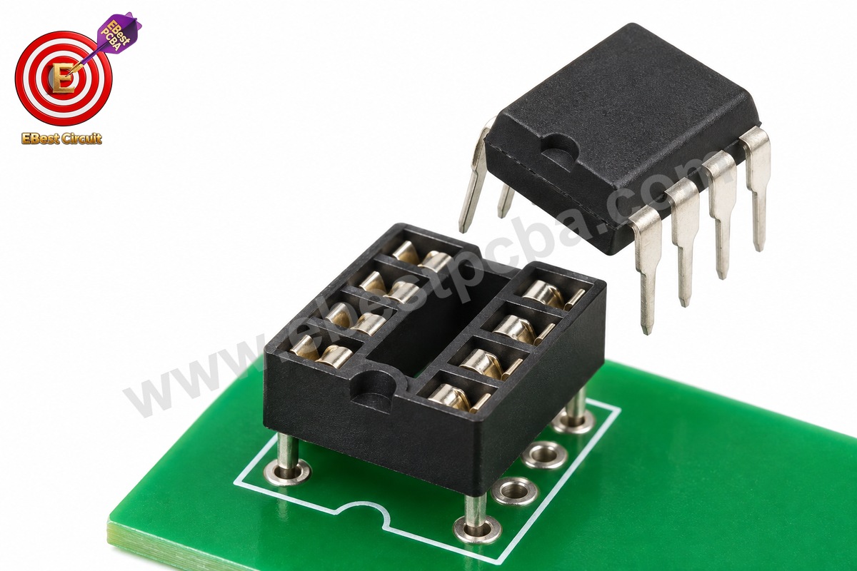
When Should You Use a Dual Inline Package Socket?
A dual inline package socket is useful when removal, replacement or repeated evaluation is part of the product’s intended use. Direct soldering is often preferable when an additional removable contact is unnecessary. The decision should consider service access, contact reliability, height and mechanical loading.
Match pin count, adjacent-contact pitch and row spacing, then review the socket manufacturer’s compatible lead range and mounting dimensions. Contact construction, plating, retention and temperature limits vary between products. A TE Connectivity DIP socket example specifies fourteen positions and a 2.54 mm centerline; that combination alone does not establish compatibility with every fourteen-pin device.
- Confirm Pin 1 orientation on both the socket and the IC.
- Include the socket’s added height in the enclosure clearance check.
- Review retention and contact requirements for the operating environment.
- Specify whether the socket is fitted during assembly and when the IC is inserted.
- Document whether the functional test applies to the final socketed configuration.
Do not force bent or misaligned leads into a socket. A lead can fold under the body while the package appears seated. For field-replaceable parts, provide clear insertion orientation and suitable handling instructions.
Dual Inline Package Uses
Dual inline package uses include breadboard development, educational electronics, serviceable designs and products that retain existing through-hole components. The package can suit work where accessible leads and replaceable devices are more valuable than the smallest board area.
Amplifiers, logic devices, controllers and optocouplers are examples of component functions available in selected DIP families. Availability depends on the exact device; a modern IC should not be assumed to have a DIP option. For a repeat-production design, review lifecycle status and approved sources before building a product around a particular package.
On a compact, dense board, a surface-mount alternative may offer a better mechanical fit. That does not make it an automatic replacement: electrical limits, pin functions and the circuit’s operating conditions still need review.
How Does DIP Compare With Surface-Mount Packages?
DIP normally uses through-hole insertion, while packages such as SOIC use surface pads. The choice changes the footprint and assembly route, even when two versions contain the same device family.
| Feature | Conventional through-hole DIP | Surface-mount IC package |
|---|---|---|
| PCB connection | Leads enter plated holes | Terminals attach to surface lands |
| Assembly route | Insertion followed by suitable soldering | Placement and suitable reflow process |
| Socket use | Matching sockets available for selected formats | Depends on specialized socket or adapter arrangements |
| Layout tradeoff | Holes and body occupy board space | Often supports denser placement, depending on package |
Compare complete part numbers rather than only the base device name. Even a pin-compatible change can alter thermal behavior, lead finish, handling needs or assembly conditions. An adapter board may help development, but its height and interconnections belong in the electrical and mechanical assessment.
What Should Be Checked Before Through-Hole Assembly?
Confirm the BOM, footprint, orientation and soldering route before releasing a DIP assembly. These inputs determine whether material receiving, board fabrication and insertion are working from the same requirements.
- Check the material. Match the manufacturer, full part number, package code and approved revision. Inspect leads and packaging condition.
- Check the footprint. Review hole positions, finished-hole requirements, annular pads and component clearance against the drawing.
- Check orientation. Align the device index, PCB Pin 1 marking and assembly drawing before insertion.
- Define soldering. Select a process appropriate to the component, board construction and mixed-technology assembly. Specify limitations from the component documentation.
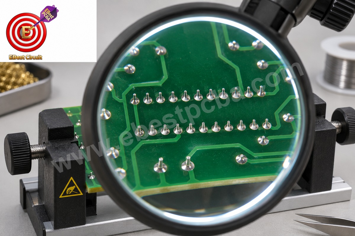
- Inspect the result. Review seating, lead condition, solder connections, bridging and other agreed workmanship criteria.
- Test the required functions. Define electrical checks, firmware, fixtures and pass/fail limits instead of relying on appearance alone.
Mixed SMT and through-hole boards need an agreed sequence. Nearby surface-mount parts, thermal mass and access can affect the through-hole operation. Rework also needs a suitable plan: a long row of pins should not be pulled from the board while some joints remain attached.
Our PCB assembly service can be reviewed against your actual board and component requirements. For purchasing questions, our component sourcing support starts with the approved manufacturer part numbers and alternate-approval requirements.
Which DIP Assembly Problems Should You Look For?
Common problems include reversed orientation, bent leads, incomplete insertion and unintended solder connections. Separate physical assembly faults from a wrong or unsuitable IC, because the corrective action is different.
| Observed problem | Relevant check |
|---|---|
| Package will not seat | Row spacing, bent leads, blocked holes and socket compatibility |
| IC is rotated | Device index, assembly drawing and PCB Pin 1 marking |
| Adjacent leads are shorted | Solder bridges, lead deformation and electrical net verification |
| Board fails its functional test | Part identity, supply connections, insertion and the specified test conditions |
A notch aligned with the silkscreen is a useful assembly check, but it is not proof that the PCB library assigned the right nets. Keep the schematic-to-footprint review separate from the operator’s insertion check.
Frequently Asked Questions
Does DIP-8 mean an eight-bit device?
No. DIP-8 refers to the package’s eight lead positions. It does not describe processing width, channel count or circuit function. Use the manufacturer’s device datasheet to identify what the IC does and how its pins are assigned.
Are DIP and DIL different package technologies?
DIP and DIL are commonly used names for the dual in-line arrangement. Terminology alone is not a footprint specification. Confirm the package drawing, lead count, dimensions and manufacturer code rather than approving a part solely because its listing uses either abbreviation.
Does every eight-pin IC fit a DIP-8 footprint?
No. An eight-pin IC may be supplied in a surface-mount package or another outline. Even among dual-row parts, check the lead spacing and body dimensions. Electrical compatibility also requires a separate comparison of pin functions and operating specifications.
Can I identify Pin 1 from any circular mark?
Not reliably. A package can have mold marks as well as an index feature. Use the exact package documentation to identify the notch, dot or other Pin 1 indicator. Also check whether the published drawing shows the top or bottom of the component.
Is the body width the same as the distance between lead rows?
No. The molded body and the lead-row geometry are separate drawing dimensions. Confusing them can produce an incompatible footprint or socket choice. Check the drawing’s dimension references and tolerances instead of measuring only the plastic body.
Can a DIP component be placed in a solderless breadboard?
Many conventional DIP ICs are convenient for breadboard work, but check pitch, row spacing, pin condition and physical fit first. The breadboard’s contacts and interconnections also have limits; a prototype connection is not automatically suitable for every current, frequency or environment.
Does a socket remove the need for orientation checks?
No. The socket can be installed with one orientation and the IC inserted with another. Document the final Pin 1 direction and check the seated device. A socket adds a removable interface; it does not change the IC’s electrical pin assignments.
Can a DIP switch replace a DIP IC?
No. A switch and an integrated circuit perform different functions even if their housings resemble each other. A DIP switch provides selectable connections. Match the schematic function, pin arrangement and ratings before considering any component replacement.
Can ceramic and plastic packages always be exchanged?
No. Similar lead counts do not establish equivalent dimensions, electrical grades or operating limits. Check the full device and package codes, the manufacturer’s drawings and the application requirements. The material label is only one part of the comparison.
What should I send for a DIP PCBA quotation?
Send PCB fabrication data, the BOM with full manufacturer part numbers, assembly drawings, quantity and test requirements. Identify sockets, customer-supplied parts and approved alternatives. Include package drawings or mechanical constraints where the footprint or enclosure fit needs clarification.
How Can We Review Your DIP Assembly Requirements?
Start with an approved component list and a footprint checked against the actual package drawing. We can then review the board, sourcing responsibility, insertion requirements and proposed inspection or test scope together.
Send your Gerber or ODB++ files, BOM, assembly drawing, quantity and testing requirements to sales@ebestpcba.com. At EBest PCBA, we will review the available manufacturing information and identify open questions before confirming the quotation and build requirements.