In an NMOS vs PMOS comparison, the key difference is gate polarity. An enhancement-mode NMOS turns on when its gate is sufficiently above its source, whereas a PMOS turns on when its gate is sufficiently below its source. Use an NMOS to switch the ground side of a load when you can interrupt its return path. A PMOS is often the simpler choice when the load must stay grounded and you need to switch its positive supply.
A 3.3 V GPIO can turn on a suitably rated NMOS with its source at ground. However, that same GPIO can fail to turn off a PMOS with its source at 5 V. The difference is the voltage between gate and source. The examples below show what to wire, what to measure, and when a high-side NMOS is worth the extra driver.
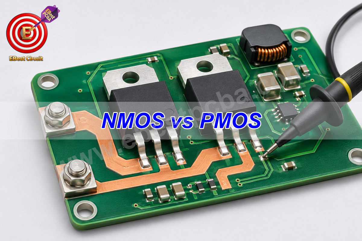
What Is the Difference Between NMOS and PMOS?
NMOS uses an electron channel and needs positive gate-to-source drive, while PMOS uses a hole channel and needs negative gate-to-source drive. These polarity rules apply to the enhancement-mode parts normally used as switches.
Each has a gate (G), drain (D) and source (S). The gate controls the channel between drain and source. The gate voltage by itself tells you little unless you know the source voltage. This matters most when the source moves, as it does on a high-side NMOS.
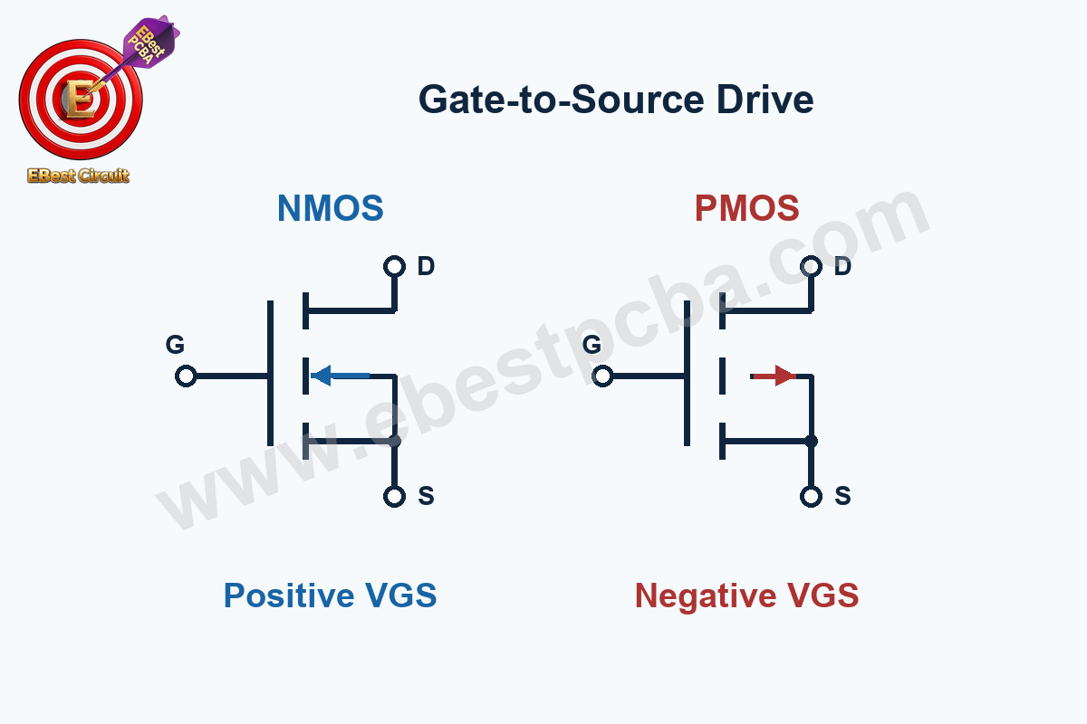
Use the symbol to trace the circuit, but check the exact part’s datasheet to identify its physical pins. The same package can contain either channel type, and a simplified symbol may omit the body diode.
| Property | NMOS | PMOS |
|---|---|---|
| Channel carriers | Electrons | Holes |
| Gate drive to turn on | Gate above source | Gate below source |
| Gate drive to turn off | Gate near source | Gate near source |
| Body diode in a typical discrete part | Anode at source, cathode at drain | Anode at drain, cathode at source |
| Common switch placement | Low side, or high side with a suitable driver | High side with a source-referenced gate circuit |
To tell them apart on a board, read the designator and pull up the BOM and datasheet. Confirm the G, D and S pins against the board nets. A PMOS gate bubble appears in some schematic styles, but its absence alone cannot identify a part. If the board and drawing disagree, start with the actual package marking and the manufacturer’s pin diagram.
What Gate Voltage Turns an NMOS or PMOS On?
An NMOS needs a sufficiently positive VGS and a PMOS needs a sufficiently negative VGS for the required load current. The datasheet’s on-resistance test voltage is a better starting point for gate-drive selection than the threshold voltage.
» VGS = VG − VS
- Grounded NMOS. With the source at 0 V and the gate at 3.3 V, VGS is +3.3 V. If maximum RDS(on) is specified only at 4.5 V and 10 V, those values do not guarantee the resistance at 3.3 V. Look for a part with a guaranteed limit at a drive the circuit can deliver.
- PMOS on a 5 V rail. With the source at 5 V and gate at 0 V, VGS is −5 V. Bringing the gate back to 5 V gives 0 V across the gate and source, which turns the channel off. A gate held at 3.3 V still leaves −1.7 V across it. Some parts can conduct at that bias.
Gate threshold is typically measured at a small drain current. As a result, an NMOS with a 1 V threshold can start to conduct long before it can carry an ampere with an acceptable voltage drop. For example, if a switch must drop less than 100 mV at 2 A, its resistance budget is 50 mΩ before allowing for the PCB and connectors. Check the device’s maximum RDS(on) at your minimum drive and allow for heating before comparing it with that budget.
Enough gate drive gets the switch on, but too much can exceed its absolute VGS rating. Pulling a PMOS gate to ground on a 24 V rail applies −24 V across gate and source, beyond a ±20 V rating. A level shifter can let the controller operate the gate, but the circuit still needs to limit steady and transient VGS.
How Do You Wire NMOS and PMOS as Load Switches?
Wire a low-side NMOS between the load and ground, or a high-side PMOS between the supply and the load. The low-side circuit switches the return path. The high-side circuit switches the positive supply and leaves the load’s ground connected.
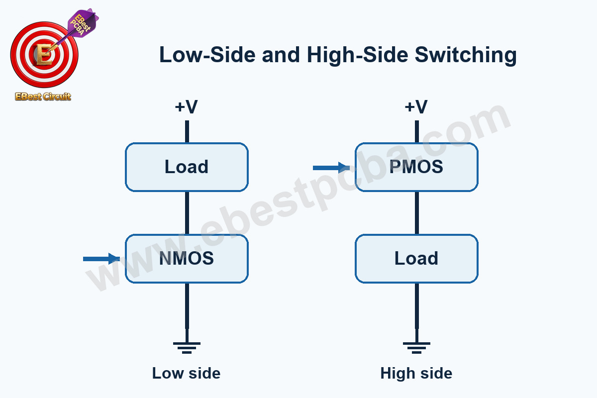
Low-side NMOS for a grounded control signal
- Connect the load between the positive rail and the drain. Connect the source to the power return.
- Drive the gate from a controller or gate driver referenced to the source. Fit a gate-to-source pull-down so the gate stays low while the controller pin is high impedance during reset.
- Power up with the actual load. Check VGS and the on-state drain-to-source drop. If you see the gate rise at the controller but not across the MOSFET’s gate and source, check the driver return and the source connection.
This layout is common for a relay coil, lamp or other load that can lose its ground connection. For a relay, a flyback diode across the coil gives current a path after turn-off. Put the cathode on the positive side and the anode on the switched side in this example. If the load also has signal cables or a chassis connection, check whether those connections create another ground path around the MOSFET.
High-side PMOS for a load that must stay grounded
- Connect source to the positive input and drain to the load. Put a pull-up between gate and source so the switch defaults off.
- Use an open-drain stage or a small control transistor to pull the gate down when the load should turn on. On a 5 V rail, pulling the gate close to ground gives nearly −5 V of drive. Check the control transistor’s voltage rating and the PMOS gate limit.
- Check startup with the supply present and the controller held in reset. The PMOS gate should settle near its source in the off state. Then enable the load and confirm the gate moves far enough below the source under real operating conditions.
A pull-up also affects turn-off time because it must recharge the gate. A weak pull-up reduces the current drawn when the gate is held low, but it may make turn-off too slow for PWM or a fast disconnect. If switching speed matters, choose a driver that can charge and discharge the gate at the required rate.
When Is a High-Side NMOS Better Than a PMOS?
A high-side NMOS makes sense when its lower resistance or better switching performance saves enough power to justify a gate driver. By contrast, a PMOS often suits a modest load that only needs occasional on/off control.
In the NMOS high-side circuit, connect the drain to the supply and the source to the load. As the source rises toward the supply, the driver must raise the gate above it. A gate fixed at the supply voltage loses drive as the source rises, so the output can stall below the rail and the MOSFET can dissipate more power than expected.
The driver’s supply method determines whether you can leave the switch on. Choose it to match the longest uninterrupted on time in your circuit.
- Bootstrap driver. It normally refreshes its capacitor when the switching node returns low. Check how long it can stay high before gate drive droops. A standard bootstrap arrangement may need periodic off time.
- Charge pump or independent floating supply. These are options when the switch must remain on continuously. Check startup behavior, pump capability and the usable gate voltage at the lowest input supply.
To see what lower resistance buys you, compare both parts at the same load using the gate drive each will actually receive. At a steady 3 A, every additional 10 mΩ adds 90 mW of conduction loss.
» Conduction loss = I2 × RDS(on)
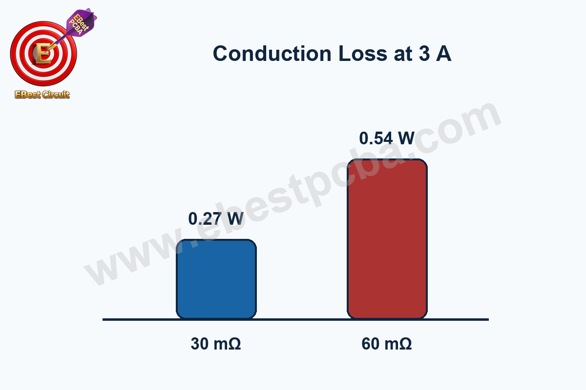
In the example, moving from 60 mΩ to 30 mΩ saves 0.27 W while the switch is on. That difference can matter in an always-on battery path, but the average savings may be small when the load runs only briefly. If the load uses PWM, switching losses, gate charge and driver current also enter the comparison. If a larger gate charge slows the transitions, the MOSFET can lose more energy while switching.
How Does the Body Diode Affect an Off MOSFET?
The body diode in a typical discrete MOSFET can conduct in one direction even when the gate has turned the channel off. Check the diode direction against every way the board can be powered.
In the high-side PMOS example, the diode runs from the load side (drain) toward the supply side (source). With the switch off, the diode blocks the normal supply-to-load direction. However, if another source powers the load and raises its voltage above the input, the diode can feed current back into the input rail. A high-side NMOS with drain at the input and source at the load has the same load-to-input diode direction.
- One supply and one load. Check the diode orientation with the normal supply present. A source and drain swap can turn the diode into an unintended path that powers the load even with VGS near zero.
- Two possible power sources. Test both with the switch disabled. For example, remove the main supply and connect the external power source on the load side. Measure the inactive rail and check for backfeed through the switch, signal interfaces or protection devices.
- Blocking both directions. Use a topology designed to block current both ways when off. Back-to-back MOSFETs have opposing body diodes. Their gate drive still has to turn both devices on and off under all relevant supply conditions.
If a disconnected rail rises on a high-impedance meter, check it under the circuit’s permitted test load. A small leakage path can produce a reading on a floating node. A diode feeding a powered rail can deliver enough current to keep other circuitry partly on. Those two cases need different fixes.
How Do NMOS and PMOS Work Together in CMOS?
A CMOS inverter uses a PMOS to pull the output toward the positive rail and an NMOS to pull it toward ground. The two gates share one input, and the two drains meet at the output.
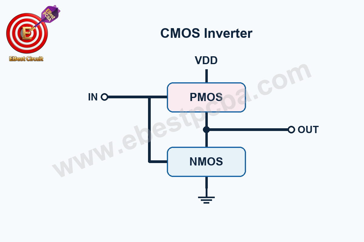
The PMOS source stays at VDD and the NMOS source stays at ground. Read each input state against those two source voltages.
| Input | Conducting device | Output |
|---|---|---|
| Low, near ground | PMOS pull-up | High, near VDD |
| High, near VDD | NMOS pull-down | Low, near ground |
In either steady logic state, one transistor drives the output. During a transition, however, both can conduct briefly. A slow input edge can extend that overlap and raise supply current. If a sensor changes voltage slowly, check the logic IC’s input transition limits and whether a Schmitt-trigger input suits the circuit.
Inside a logic IC, a designer can size the PMOS and NMOS differently to balance pull-up and pull-down drive. Electron mobility generally favors the NMOS for comparable devices, but the finished inverter’s rise and fall times also depend on device sizing and load capacitance. You cannot predict which output edge is faster from channel type alone.
How Do You Choose and Check a MOSFET for a PCB?
Choose a MOSFET that meets the circuit’s voltage, gate-drive and heat limits, then verify the exact footprint and test it on the board.
Compare these ratings using the lowest available gate drive and the highest expected load and temperature.
| Datasheet item | What to check |
|---|---|
| VDS and VGS limits | Allow for supply spikes and gate overshoot. |
| Maximum RDS(on) | Use the value at your gate drive and account for higher resistance when hot. |
| Gate charge | For PWM, check whether the driver can switch the gate fast enough. |
| Safe operating area (SOA) | For capacitive loads, check the startup current, voltage across the MOSFET and pulse duration together. |
- Before assembly: Match the gate, drain, source and exposed pad to the exact package drawing.
- At first power-up: Verify that the load stays off during reset. Under the intended load, measure the on-state voltage drop and check the temperature.
For a board review, send the schematic, Gerbers, BOM and load requirements. See our DFM report example and PCB assembly service.
NMOS vs PMOS FAQ: How Does Channel Type Affect Other Circuits?
Channel type affects gate drive in power converters, signal range in analog switches, and voltage headroom in regulators and amplifier inputs.
- Why do buck converters often use NMOS switches?
-
An NMOS often gives a buck converter lower on-resistance for a comparable voltage rating and die size. A synchronous buck can use an NMOS in both positions, with a driver that lifts the upper gate above the switch node. When comparing parts, also check gate charge and switching loss at the converter’s frequency. The lowest resistance can be a poor trade if the driver spends too long moving the gate.
- Is a PMOS LDO less stable than an NMOS LDO?
-
Channel type alone does not determine LDO stability. The pass element changes the loop behavior, but the regulator’s compensation, load current, output capacitance and capacitor ESR determine its usable operating range. Follow the selected regulator’s capacitor requirements. If it specifies a minimum effective capacitance, allow for ceramic capacitor derating at the actual output voltage.
- Why does a CMOS transmission gate use both NMOS and PMOS?
-
An NMOS passes voltages near ground well, but its gate drive falls as the signal approaches the positive rail. A PMOS has the opposite strength. A transmission gate puts both devices in parallel and drives them with complementary control signals, so the two channels cover more of the signal range. Check the analog switch’s allowed signal range and on-resistance over that range.
- When does a PMOS make sense for reverse-battery protection?
-
A PMOS can suit a moderate-current high-side protection circuit when its on-state drop is lower than the drop of a series diode. Use the orientation specified for reverse-battery protection. Its body diode must block a reversed battery with the gate off. If another source can energize the protected rail, test that condition separately, because reverse-battery protection and reverse-current blocking are different jobs.
- Why would an op amp use a PMOS input pair?
-
A PMOS input pair can help a CMOS op amp accept signals close to its negative supply in a conventional input stage. The rest of the design still determines the usable input range. Some rail-to-rail designs use both PMOS and NMOS input pairs. If accuracy near a rail matters, check common-mode limits and offset over the signal range, rather than inferring them from channel type.