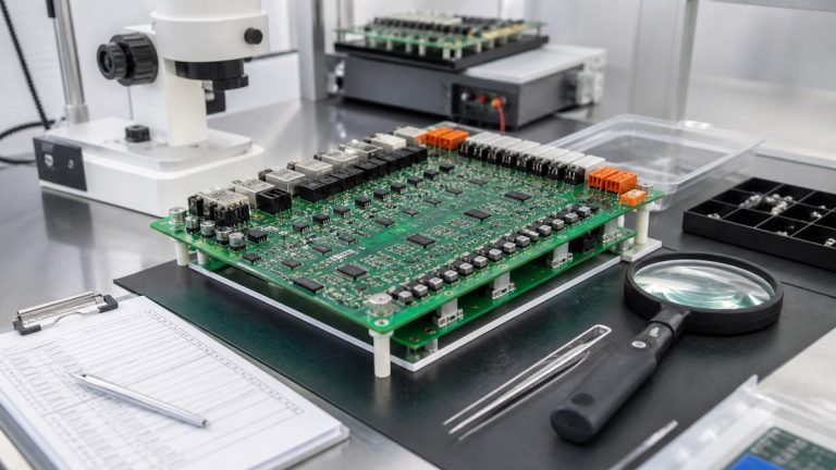
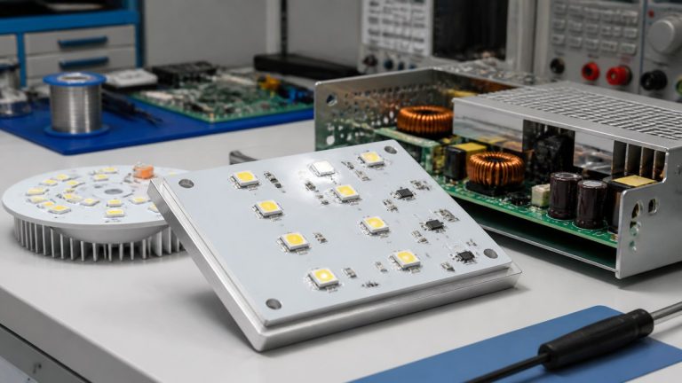
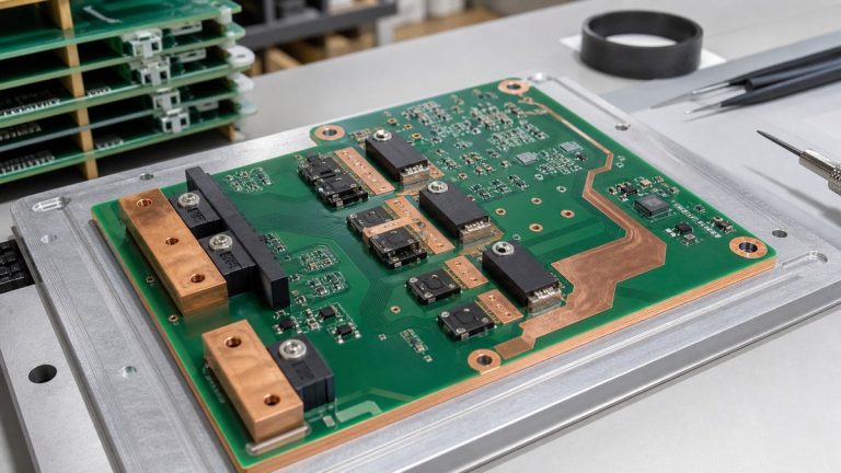
We review power-electronics PCB layouts for fabrication, assembly, inspection and test before release. Our engineers focus on features where production can alter electrical or thermal intent: copper thickness, current paths, plated holes, isolation, exposed pads, heat sinks, power terminals and high-mass components.
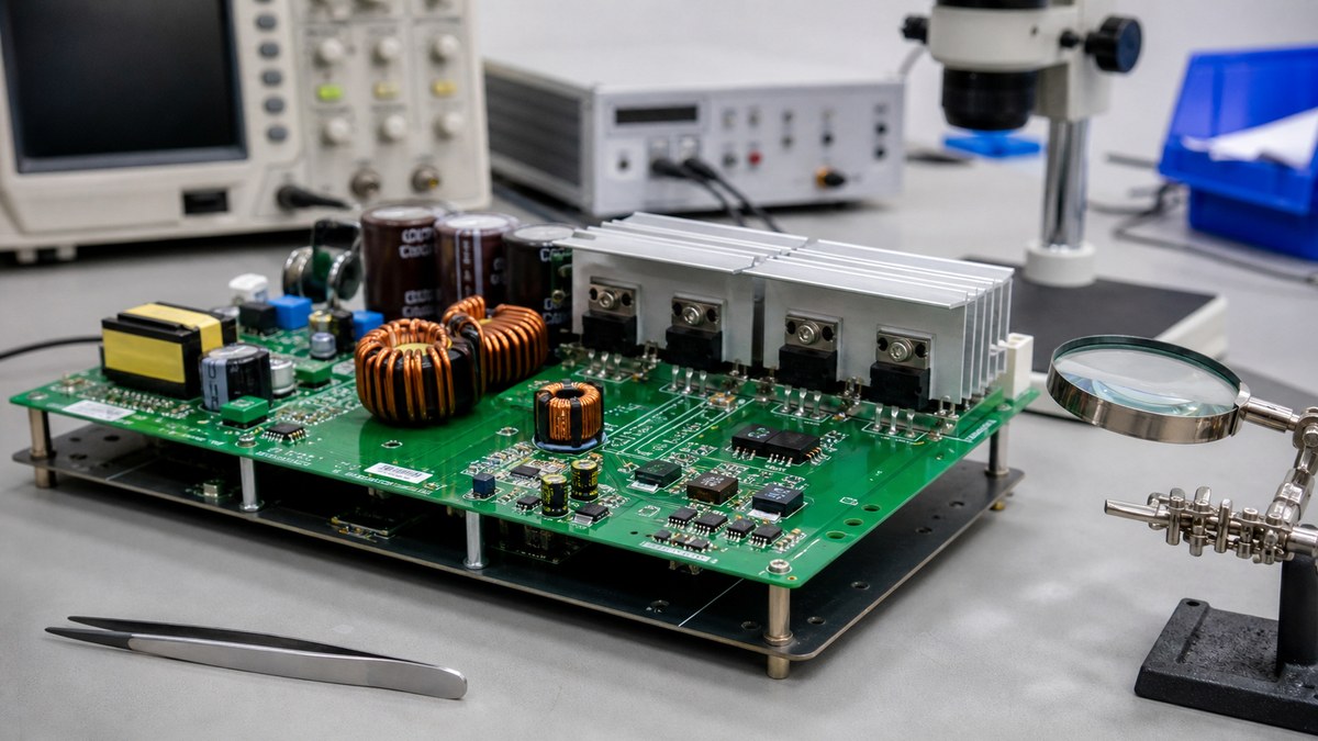
You receive specific DFM questions and an approved construction tied to the released revision. We do not redesign the converter or validate system safety; we ensure the specified physical features are buildable, inspectable and repeatable.
Power PCB DFM Map
| Area | What we review | Output |
|---|---|---|
| Copper and stack-up | Layer, base and finished copper, spacing and thickness | Approved construction |
| Current transfer | Vias, holes, pads, terminals and bus connections | Manufacturing-risk response |
| Isolation | Creepage, clearance, slots, edges and coating boundaries | Controlled geometry |
| Thermal path | Exposed pads, thermal vias, heat sinks and interfaces | Process and inspection plan |
| Assembly and test | Thermal mass, access, fixtures, loads and limits | Build and evidence route |
We Reconcile Every Definition of Copper
We compare the stack-up, fabrication drawing and image data for layer-specific copper. Starting foil, plated contribution and finished copper must not be mixed. Minimum trace and spacing must be compatible with the approved copper.
If the requested construction conflicts with fine features or board thickness, we return the trade-off before release.
Current Paths Include Vias, Holes and Joints
We review trace and plane geometry, via quantity and size, plated-hole requirements, annular rings, terminals, shunts and solder joints. A wide copper plane can still be limited by an undefined interlayer or connector transition.
Applicable structural and assembly evidence is assigned to the features manufacturing can verify. Electrical current capability remains validated by the design owner.
High-Voltage Spacing Needs a Clear Design Basis
We ask for working voltage, environment, material group, coating condition and applicable safety requirement when these affect the PCB. We then review specified creepage, clearance, slots, cutouts, board edges and component placement against process tolerance.
We preserve the approved spacing and flag features where copper, drill, routing or mask variation could reduce it.
Thermal Features Must Be Buildable and Inspectable
We review thermal-via diameter and treatment, exposed-pad geometry, paste segmentation, heat-sink holes, flatness and interface materials. These features influence both heat transfer and solder formation.
SPI, AOI, X-ray or dimensional checks are selected according to the manufacturing risk. They do not replace operating thermal validation.
Power Components Affect the Soldering Route
Large packages, transformers, inductors, capacitors and terminals create uneven thermal mass. We review reflow, selective or manual soldering needs, fixtures, component temperature limits and inspection access.
The intended production construction is used to establish the process rather than relying on a lighter prototype board.
Mechanical Interfaces Need Controlled Data
We check heat sinks, busbars, high-force connectors, mounting holes, hardware, torque inputs and enclosure keep-outs where provided. Mechanical load can affect solder joints and board flatness.
Approved materials and assembly instructions remain with the product baseline.
Test Access Must Match the Power Function
We review programming, low-voltage checks, power-up sequence, sensing, gate-drive, communication and load-test requirements. Fixtures, firmware, input conditions, loads, limits and safety controls must be defined.
Our report states the functions and conditions tested so the evidence is not mistaken for full system qualification.
Why Customers Use Our Power PCB Review
We connect high-current, high-voltage and thermal features to fabrication and assembly controls before tooling. Your team receives actionable decisions and evidence for the manufactured construction.
This reduces late changes and prevents one strong feature, such as heavy copper, from hiding a weak transition elsewhere.
Send Your Power PCB Layout for Review
Send Gerber or ODB++, stack-up, fabrication drawing, copper definitions, BOM, CPL, assembly and mechanical drawings, current, voltage, thermal conditions, isolation requirements and test procedure to sales@ebestpcba.com.
We will return DFM questions, the proposed route and evidence available.
What to Include in Your Power PCB Review Package
Send us the Gerber or ODB++ data, stack-up, copper requirement, fabrication drawing, BOM, placement data, mechanical drawing and electrical or load-test criteria. Mark the current paths, voltage domains, thermal interfaces and safety-critical spacing. We can then give your engineers specific manufacturability feedback tied to the real product instead of a generic checklist.