
How We Match High-Frequency PCB Materials to Circuit Requirements
See how We review high-frequency PCB materials, stack-ups, copper, vias, finishes and test evidence against the customer
Read article →Find practical guidance on PCB layout, DFM, materials, manufacturing, assembly, testing, and reliability. Use each article to clarify project requirements before quotation or production release.
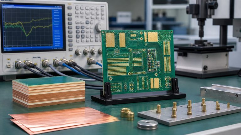
See how EBest turns PCB stack-up and impedance requirements into approved materials, dielectric, copper, geometry, coupons and production reports.
Read article →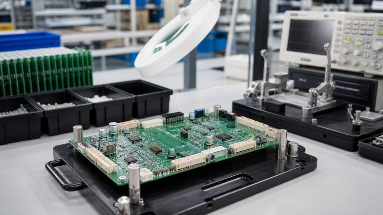
See how we control PCB assembly from released data and component sourcing through soldering, inspection, testing, traceability and shipment records.
Read article →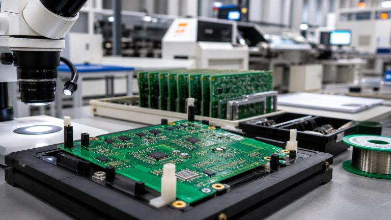
See how EBest uses customer data, CAM and DFM checks, assembly programs and production records to control PCB and PCBA manufacturing risk.
Read article →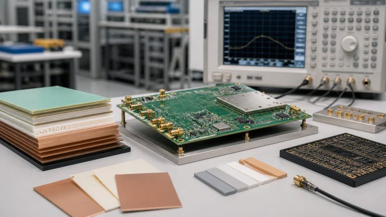
See how We review high-frequency PCB materials, stack-ups, copper, vias, finishes and test evidence against the customer
Read article →See how EBest turns PCB stack-up and impedance requirements into approved materials, dielectric, copper, geometry, coupons and production reports.
Read article →See how we control PCB assembly from released data and component sourcing through soldering, inspection, testing, traceability and shipment records.
Read article →See how EBest uses customer data, CAM and DFM checks, assembly programs and production records to control PCB and PCBA manufacturing risk.
Read article →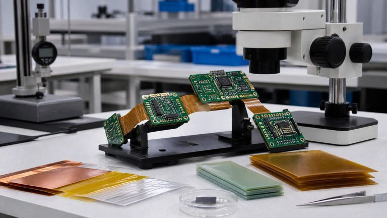
See how We review rigid-flex laminates, flex films, copper, coverlay, adhesives and stiffeners against bend, assembly and production requirements.
Read article →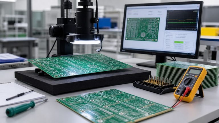
See how EBest plans PCB continuity, isolation, impedance, dimensional and structural testing and connects reports to the released bare-board lot.
Read article →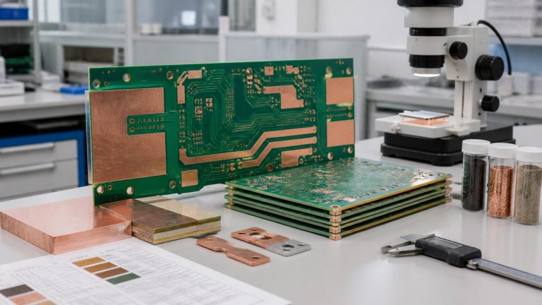
Prepare a heavy-copper PCB RFQ with clear finished copper, stack-up, geometry, via, current, thermal, soldering and inspection requirements for EBest.
Read article →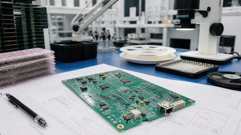
Prepare an accurate PCB or PCBA RFQ with Gerber, stack-up, drawing, BOM, CPL, assembly, mechanical, test and quality requirements.
Read article →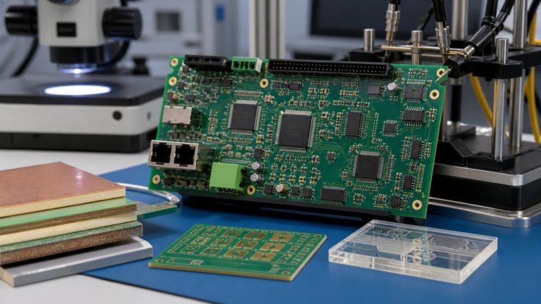
Learn how copper, laminate, prepreg, solder mask, surface finish, flex materials and metal cores form a PCB, and how we select the build.
Read article →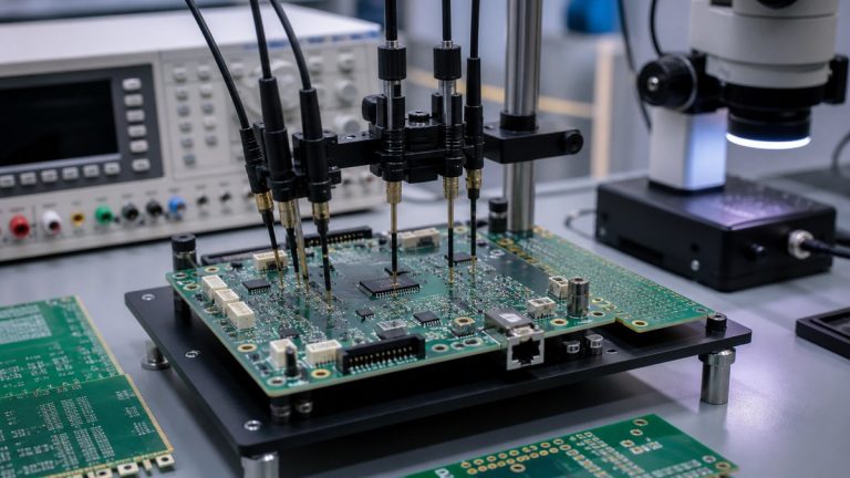
Compare bare-board electrical test, impedance, AOI, X-ray, ICT, flying probe and functional testing, including what each method proves.
Read article →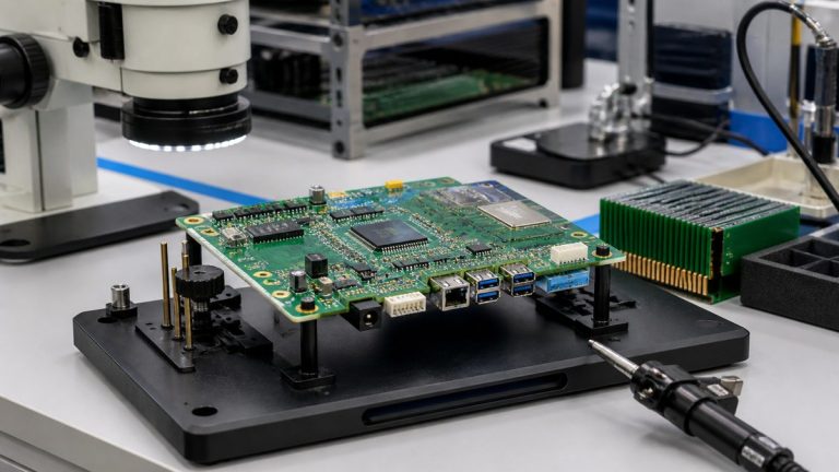
See how we turn Gerber, BOM, CPL, drawings and test requirements into a controlled PCB fabrication and PCBA production route.
Read article →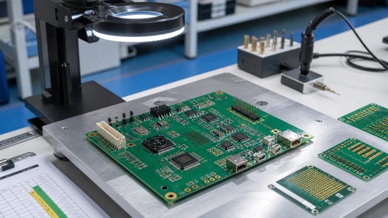
Use this PCB and PCBA DFM checklist to prepare fabrication, assembly, BOM, mechanical, inspection and test data before build.
Read article →Send the files and requirements you already have. EBest PCBA will help separate general guidance from the construction, sourcing, inspection and test decisions required for your build.
The Blog helps users understand technical decisions. Project capability, tolerance, price and schedule are still confirmed from the released files.