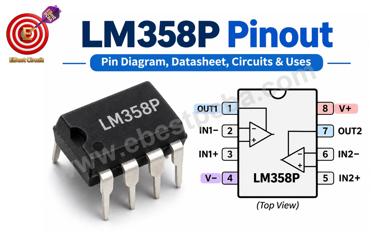
The LM358P pinout consists of 8 pins for 2 independent operational amplifiers in a single PDIP-8 package. Pins 1–3 belong to amplifier 1, Pins 5–7 belong to amplifier 2, Pin 4 connects to the negative supply (V−), and Pin 8 connects to the positive supply (V+). The LM358P is commonly used for sensor signal conditioning, voltage monitoring, low-frequency amplification, and general analog circuits. This guide covers its pin configuration, datasheet specifications, wiring diagrams, amplifier circuits, typical uses, and LM358N compatibility.
At EBest PCBA, we support PCB fabrication, component sourcing, SMT/DIP assembly, inspection, and functional testing for analog electronic products. Our capabilities include Free DFM, No MOQ, 4 SMT lines, and MES single-board traceability. With 1 sales representative and 3 engineers coordinating each project’s technical requirements, we help customers review component footprints, BOM accuracy, and assembly conditions before manufacturing. Send your Gerber files, BOM, quantities, and testing requirements to sales@ebestpcba.com for a project-specific PCB assembly review and quotation.
Key Takeaways
-
The LM358P is a dual operational amplifier containing 2 independent amplifier channels in an 8-pin PDIP package, suitable for many low-frequency analog applications.
-
The standard LM358P pinout uses Pins 1–3 for amplifier 1 and Pins 5–7 for amplifier 2. Pin 4 is V−, and Pin 8 is V+.
-
The classic Texas Instruments LM358P supports a total supply voltage of 3–30 V, allowing single-supply and suitable dual-supply configurations.
-
The LM358P input common-mode range includes the negative supply rail, making it useful for measuring signals near ground in single-supply circuits.
-
LM358P is not a rail-to-rail output amplifier. Its output can approach the negative rail under suitable loading but requires significant headroom below the positive supply.
-
The LM358P has a typical gain-bandwidth product of 0.7 MHz and a slew rate of 0.3 V/µs, making it more suitable for low-frequency signal processing than high-speed applications.
-
LM358P and corresponding LM358N versions can share the same functional 8-pin arrangement, but manufacturer specifications, package dimensions, and approved part numbers must be checked before replacement.
-
Reliable LM358P PCB assembly requires correct Pin 1 orientation, PDIP-8 footprint selection, power decoupling, feedback routing, and electrical testing to verify the assembled circuit.
What Is the LM358P Pinout and Pin Configuration?
The LM358P is an 8-pin dual operational amplifier with 2 independent amplifiers sharing the same power supply. Each amplifier has a non-inverting input, an inverting input, and an output. The standard LM358P pinout follows the common dual-op-amp configuration used in many general-purpose analog circuits.
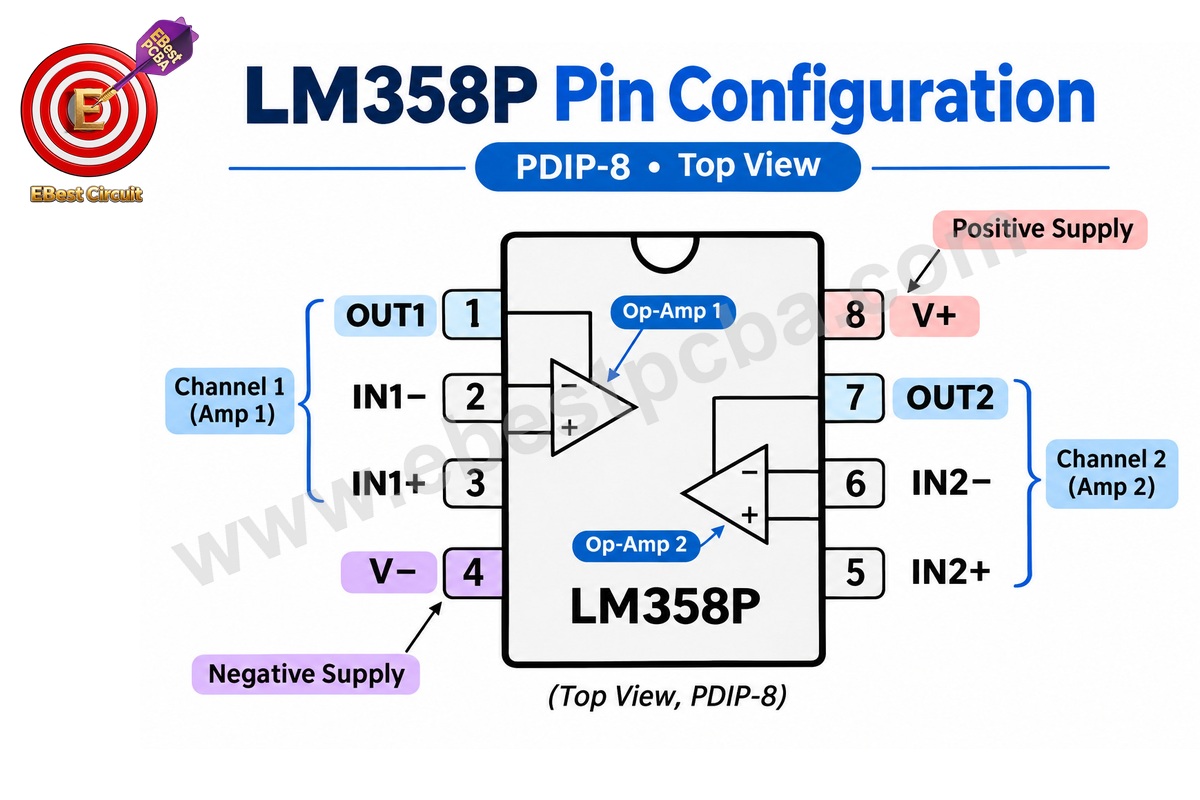
The following diagram shows the IC from the top, with the package notch facing upward.
LM358P Pinout Diagram — Top View
               LM358P
           ┌─────∪─────┐
    OUT1  1│           │8  V+
    IN1−  2│           │7  OUT2
    IN1+  3│           │6  IN2−
      V−  4│           │5  IN2+
           └───────────┘
LM358P Pin Functions
| Pin | Pin Name | Function |
|---|---|---|
| 1 | OUT1 | Amplifier 1 output |
| 2 | IN1− | Amplifier 1 inverting input |
| 3 | IN1+ | Amplifier 1 non-inverting input |
| 4 | V− | Negative supply / GND |
| 5 | IN2+ | Amplifier 2 non-inverting input |
| 6 | IN2− | Amplifier 2 inverting input |
| 7 | OUT2 | Amplifier 2 output |
| 8 | V+ | Positive supply |
Amplifier 1: Pins 1–3
Amplifier 1 processes the voltage difference between Pins 2 and 3, with the resulting output available at Pin 1.
-
Pin 1 (OUT1): Output of amplifier 1.
-
Pin 2 (IN1−): Inverting input, commonly connected to a feedback network.
-
Pin 3 (IN1+): Non-inverting input, commonly connected to the signal source.
Amplifier 2: Pins 5–7
Amplifier 2 operates independently of amplifier 1 while sharing the supply connections.
-
Pin 5 (IN2+): Non-inverting input.
-
Pin 6 (IN2−): Inverting input.
-
Pin 7 (OUT2): Output of amplifier 2.
Power Supply: Pins 4 and 8
-
Pin 4 (V−): Negative supply terminal. Connects to GND in a single-supply circuit or to a negative voltage in a dual-supply circuit.
-
Pin 8 (V+): Positive power supply terminal.
For example, with a 5 V single supply, Pin 8 connects to +5 V and Pin 4 connects to GND.
How to Identify Pin 1 on the LM358P
The PDIP-8 package normally has a notch or molded orientation marker. Viewed from above with the notch at the top, Pin 1 is at the upper-left corner. Pin numbering proceeds counterclockwise.
Always confirm the orientation against the manufacturer’s package drawing before PCB installation.
What Are the Key Specifications in the LM358P Datasheet?
The LM358P is a bipolar-input dual operational amplifier designed for general-purpose analog circuits. The classic Texas Instruments LM358P operates from a total supply voltage of 3–30 V and provides a typical 0.7 MHz gain-bandwidth product and 0.3 V/µs slew rate.
The following specifications apply to the classic TI LM358 series. Other versions, including LM358B and products from different manufacturers, may have different characteristics.
| Parameter | LM358P Specification |
|---|---|
| Amplifier Channels | 2 |
| Package | PDIP-8 |
| Input Architecture | Bipolar |
| Supply Voltage | 3–30 V total |
| Gain-Bandwidth Product | 0.7 MHz typical |
| Slew Rate | 0.3 V/µs typical |
| Input Offset Voltage | 7 mV maximum at 25°C |
| Quiescent Current | 0.35 mA typical per channel |
| Input Common-Mode Range | Includes V− |
| Output Swing | Non-rail-to-rail |
| Operating Temperature | 0°C to +70°C |
Specifications are based on the Texas Instruments classic LM358 product information. Individual parameters are measured under specified test conditions.
1. Single-Supply Operation
A major advantage of the classic LM358P is its ability to operate with a single positive supply.
For example, a 5 V system can power the device through:
-
Pin 8: +5 V
-
Pin 4: GND
The internal input stage supports a common-mode voltage range extending to the negative supply rail.
This makes the LM358P useful for measuring signals near ground, including low-side sensing and low-frequency voltage monitoring.
2. Input Common-Mode Voltage Range
The input common-mode range defines the input voltage region in which the amplifier operates as specified.
For the classic LM358, the range includes V− but does not reach V+.
A useful first approximation at normal conditions is:
VCM ≈ V− to (V+ − 1.5 V)
The exact range and guaranteed limits depend on supply voltage, temperature, and the applicable datasheet conditions.
For example, a circuit powered from 0–5 V should not assume that an input approaching 5 V remains within the valid common-mode range.
3. Output Voltage Swing
The LM358P output can approach the negative rail under suitable load conditions. However, it cannot generally swing all the way to the positive supply voltage.
For a 5 V circuit, the output high-level limit depends on the load and operating conditions.
Designers must check the output swing specification when connecting the amplifier to an ADC, comparator input, transistor driver, or other circuit requiring a particular voltage level.
4. Gain-Bandwidth Product
The typical gain-bandwidth product is 0.7 MHz.
A simplified relationship between closed-loop gain and bandwidth is:
BW ≈ GBWAv
For a closed-loop gain of 10:
BW ≈ 700 kHz10 = 70 kHz
This is a first-order estimate for a suitable amplifier configuration. Actual performance depends on the feedback network, load, and frequency response.
5. Slew Rate
The typical slew rate of 0.3 V/µs limits how rapidly the output can change.
For a sinusoidal signal, the minimum required slew rate is:
SR ≥ 2πfVpeak
For a 10 kHz sine wave with a 2 V peak amplitude:
SR ≥ 2π × 10,000 × 2
SR ≥ 0.126 V/μs
This is below the nominal 0.3 V/µs slew-rate specification, although signal distortion, bandwidth, temperature, and loading still require consideration.
6. LM358P vs LM358B Specifications
Texas Instruments also offers the LM358B, an updated device with improved performance.
| Specification | Classic LM358 | LM358B |
|---|---|---|
| Maximum Total Supply | 30 V | 36 V |
| Typical GBW | 0.7 MHz | 1.2 MHz |
| Typical Slew Rate | 0.3 V/µs | 0.5 V/µs |
| Input Offset | Original specification | Improved specification |
These specifications should be checked against the exact orderable device before choosing an alternative.
Official Datasheet: Texas Instruments LM358 datasheet (SLOS068)
How Do You Wire the LM358P with Single and Dual Power Supplies?
The LM358P supports both single-supply and dual-supply wiring, provided the voltage between Pins 8 and 4 remains within the device’s specified range. Pin 8 connects to the positive supply, while Pin 4 connects to the negative supply or ground.
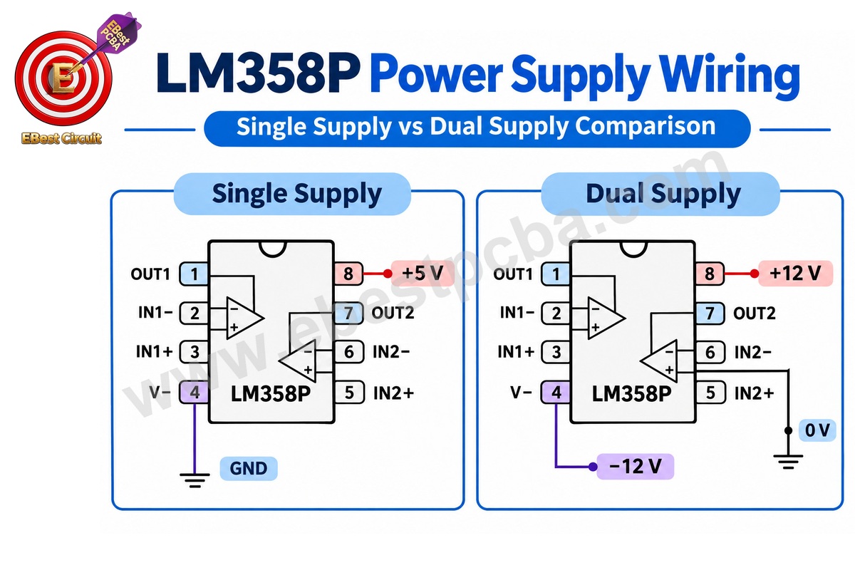
The 0 V label in the split-supply illustration marks the signal reference. Use the wiring table below for the supply connections. Connect amplifier inputs according to your circuit.
The supply configuration affects the available input common-mode range and output voltage swing.
1. LM358P Single-Supply Wiring
A 5 V single-supply circuit uses the following connections:
| Connection | LM358P Pin |
|---|---|
| +5 V | Pin 8 |
| GND | Pin 4 |
| Amplifier 1 Input (+) | Pin 3 |
| Amplifier 1 Input (−) | Pin 2 |
| Amplifier 1 Output | Pin 1 |
For amplifier 2, use Pins 5, 6, and 7.
A single supply is convenient for many sensor circuits, battery-powered electronics, and embedded control boards.
However, the input voltage and desired output must remain within the amplifier’s usable operating range.
2. LM358P Dual-Supply Wiring
A dual-supply circuit may use +12 V and −12 V.
Typical connections are:
-
Pin 8 → +12 V
-
Pin 4 → −12 V
-
Signal reference → 0 V
The total supply voltage is:
VS = V+ − V−
VS = 12 − (−12) = 24 V
This is within the classic LM358’s supported total supply range.
Dual-supply operation can be useful when the analog signal must move above and below a 0 V reference.
3. Power Supply Decoupling
Appropriate power decoupling helps limit supply disturbances.
For a typical PCB design:
-
Place a 100 nF ceramic bypass capacitor close to the supply pins.
-
Keep the supply and return connections short.
-
Add bulk capacitance where needed by the power distribution network.
-
Review nearby switching circuits and high-current return paths.
A dual-supply design may use decoupling from each rail to the appropriate reference, according to the circuit’s power architecture.
4. Input and Output Connection Checks
Before powering the board, verify that the inputs remain within the permitted operating range and that the load does not demand more output current or voltage swing than the amplifier can provide.
If only 1 amplifier channel is used, the second amplifier should be placed in a stable configuration.
A common approach is to connect the unused channel as a voltage follower with its non-inverting input biased to a valid reference voltage.
How to Build an LM358P Amplifier Circuit Diagram?
An LM358P amplifier circuit uses negative feedback to establish a controlled voltage gain. Common arrangements include non-inverting amplifiers, inverting amplifiers, and voltage followers.
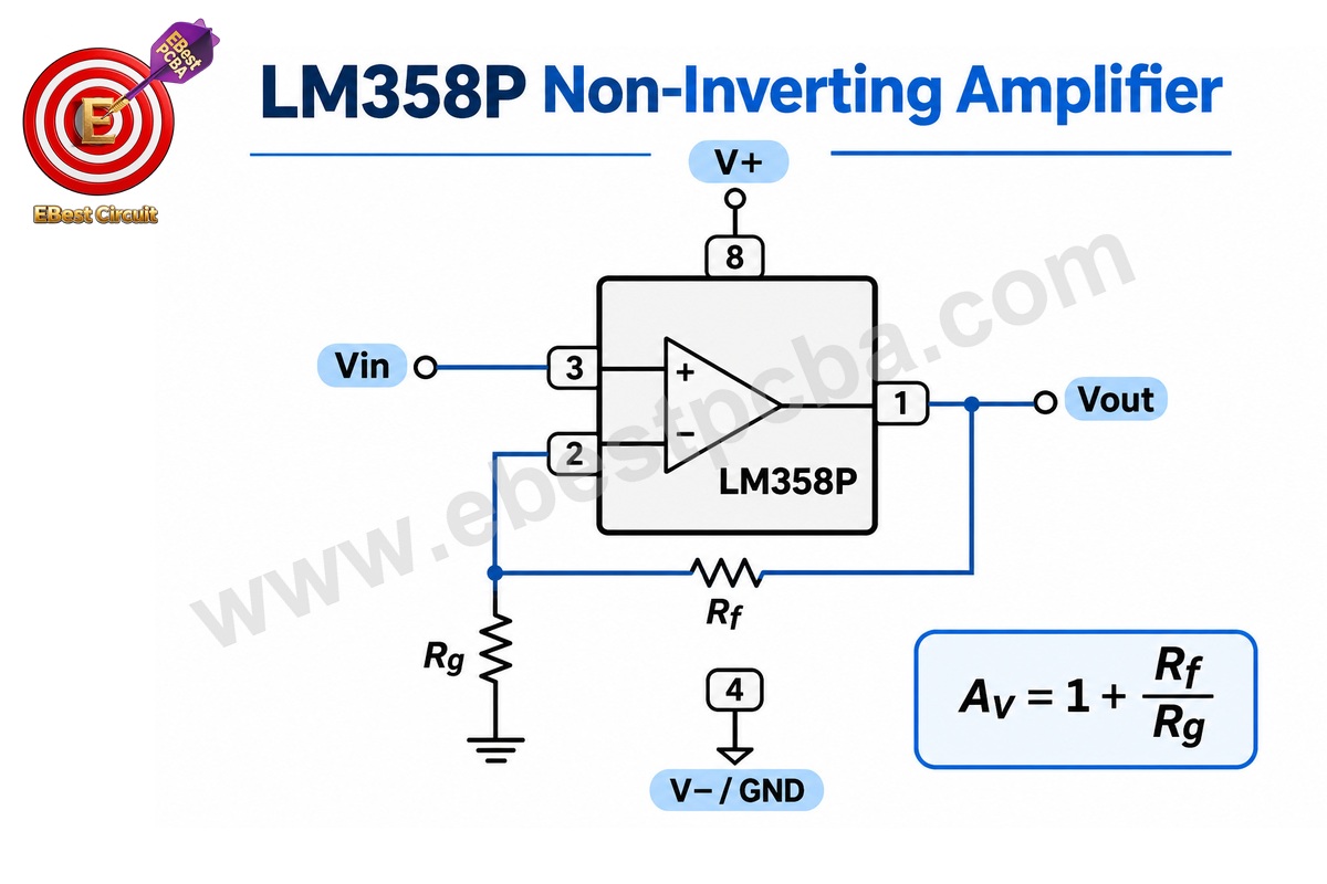
The 2 amplifier channels can be configured independently, allowing one LM358P IC to process 2 separate signals.
1. Non-Inverting Amplifier Circuit
A non-inverting amplifier produces an output signal with the same polarity as the input.
For amplifier 1, the connections are:
-
Pin 3 → Signal input.
-
Pin 2 → Feedback node.
-
Pin 1 → Signal output.
-
Pin 8 → Positive supply.
-
Pin 4 → Negative supply or GND.
Connect feedback resistor (R_f) between Pin 1 and Pin 2. Connect resistor (R_g) from Pin 2 to the appropriate reference voltage.
The ideal closed-loop gain is:
Av = 1 + RfRg
For example:
Rf = 20 kΩ, Rg = 10 kΩ
Av = 1 + 2010 = 3
If the input is 0.5 V relative to the reference, the ideal output is 1.5 V relative to that reference, provided both input and output remain within the valid operating ranges.
2. Voltage Follower Circuit
A voltage follower provides a nominal gain of 1 and is often used as a buffer between a signal source and another circuit stage.
Using amplifier 2:
-
Connect the input signal to Pin 5.
-
Connect Pin 7 directly to Pin 6.
-
Take the output from Pin 7.
The ideal voltage gain is:
Av = 1
This configuration can help reduce loading on relatively high-impedance signal sources.
However, LM358P input bias current and other nonideal characteristics must be considered in precision applications.
3. Inverting Amplifier Circuit
An inverting amplifier produces an output with opposite polarity relative to the chosen reference.
For amplifier 1:
-
Connect the input through (R_{in}) to Pin 2.
-
Connect (R_f) between Pin 1 and Pin 2.
-
Connect Pin 3 to a suitable reference voltage.
-
Take the output from Pin 1.
The ideal gain is:
Av = −RfRin
If both resistors are 10 kΩ:
Av = −10 kΩ10 kΩ = −1
With a suitable dual supply, the circuit can invert a signal around a 0 V reference.
For a single-supply arrangement, the reference and input bias conditions must be selected so that the required output remains within the amplifier’s operating range.
Which LM358P Circuit Should You Choose?
| Circuit | Ideal Gain | Typical Use |
|---|---|---|
| Non-inverting | Positive, ≥1 | Signal amplification |
| Inverting | Negative | Signal inversion |
| Voltage follower | 1 | Signal buffering |
The final design should account for common-mode voltage, output loading, feedback stability, noise, and available bandwidth.
What Are the Common LM358P Uses and Applications?
The LM358P is commonly used in low-frequency analog amplification, sensor signal conditioning, voltage monitoring, and threshold detection. Its single-supply capability and ground-sensing input range make it suitable for many control and measurement circuits.
The most practical applications depend on the required signal frequency, voltage range, accuracy, and load.
1. Sensor Signal Conditioning
The LM358P can amplify low-frequency voltage signals produced by sensors.
For example, a sensor may generate a voltage ranging from 0.1 V to 0.5 V.
A properly designed non-inverting amplifier can increase the signal amplitude before it reaches an ADC or monitoring circuit.
Before selecting the gain, engineers should verify:
-
Sensor output impedance.
-
Expected signal range.
-
Input offset and bias current.
-
Output voltage requirements.
-
Supply voltage and available headroom.
The LM358P is useful for general-purpose sensing, but precision applications may require a lower-offset or lower-drift amplifier.
2. Voltage Monitoring
LM358P can support circuits that monitor battery voltage, supply voltage, or other low-frequency electrical signals.
A resistor divider can scale a higher voltage into a range suitable for the amplifier input.
A buffer or amplifier may then provide a signal for further processing.
For systems that require accurate measurements, the resistor tolerance, amplifier offset, supply conditions, and ADC reference must be considered together.
3. Threshold Detection
An LM358P can be configured to respond when an input voltage passes a reference threshold.
For example, an indicator circuit may compare a measured voltage with a selected reference and change its output state when the threshold is crossed.
However, LM358P is an operational amplifier rather than a dedicated comparator.
Important limitations include:
-
Output saturation recovery.
-
Switching speed.
-
Input common-mode limits.
-
Output voltage swing.
-
Possible unstable switching near the threshold.
For circuits requiring fast or precise switching, a dedicated comparator such as an appropriate LM339-family device may be a better choice.
4. LM358P Audio Amplifier
The LM358P can amplify small audio-frequency signals when the required gain, amplitude, and bandwidth are within its capabilities.
Possible applications include:
-
Basic audio signal conditioning.
-
Low-frequency audio preamplification.
-
Audio level sensing.
-
Simple experimental sound circuits.
Its 0.3 V/µs typical slew rate, 0.7 MHz gain-bandwidth product, and output-stage characteristics limit its performance compared with purpose-designed audio amplifiers.
In particular, LM358P is not intended to directly drive a typical low-impedance loudspeaker as an audio power amplifier.
For higher-quality audio signal paths, engineers should compare noise, distortion, input bias current, bandwidth, and output-drive requirements against dedicated audio op amps.
LM358P vs LM358N: Are Their Pinouts the Same?
LM358P and corresponding standard 8-pin LM358N variants generally use the same functional pin arrangement, with Pins 1–3 serving amplifier 1, Pins 5–7 serving amplifier 2, and Pins 4 and 8 providing the power connections.
However, the suffix and package designation depend on the manufacturer. Electrical and mechanical compatibility must be confirmed using the complete part number.
| Feature | TI LM358P | LM358N / LM358-N |
|---|---|---|
| Amplifier Channels | 2 | 2 |
| Standard Pinout | Dual-op-amp 8-pin | Dual-op-amp 8-pin |
| Package | PDIP-8 | Verify exact MPN |
| Electrical Specs | Classic TI LM358 | Manufacturer-specific |
| Substitution | Requires verification | Requires verification |
1. LM358P Pinout
Texas Instruments LM358P is a specific orderable device in the classic LM358 family.
The P suffix identifies its PDIP package option.
It uses the standard dual-amplifier 8-pin configuration.
2. LM358N Pinout
LM358N designations commonly appear on versions from other manufacturers or historical product families.
A corresponding 8-pin version can use the same functional pinout, but the package dimensions, temperature grade, electrical specifications, and product qualification may differ.
Texas Instruments also maintains an LM358-N product family, which should be evaluated according to its own documentation rather than treated as universally identical to every LM358N device.
3. Can LM358N Replace LM358P?
Replacement may be possible if the selected components meet the circuit’s electrical and mechanical requirements.
Check the following before approval:
-
Manufacturer and exact MPN.
-
Package dimensions and lead spacing.
-
Functional pin arrangement.
-
Supply voltage limits.
-
Input common-mode range.
-
Offset voltage and bias current.
-
Output swing and load capability.
-
Temperature grade.
For an existing PCB, matching the pinout is only one part of the replacement process.
A change in electrical specifications may require circuit validation even when both parts fit the same socket or footprint.
Can LM324 or LM386 Replace the LM358P?
LM324 and LM386 are not direct pin-compatible replacements for LM358P. Although their model numbers are similar, the devices serve different functions or use different pin configurations.
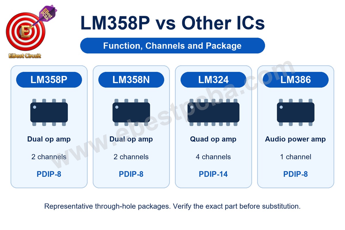
The LM324 is a 4-channel operational amplifier, while LM386 is an audio power amplifier.
| IC | Device Type | Channels | Common Package |
|---|---|---|---|
| LM358P | Operational amplifier | 2 | PDIP-8 |
| LM324 | Operational amplifier | 4 | DIP-14 |
| LM386 | Audio power amplifier | 1 | DIP-8 |
1. LM324 vs LM358P
LM324 contains 4 operational amplifier channels rather than 2.
Both devices are widely used in general-purpose low-frequency analog circuits, and some versions share related design characteristics.
However, a standard LM324 DIP-14 package has 14 pins, while LM358P uses PDIP-8.
The two packages are not directly interchangeable on the same PCB footprint.
If a circuit requires more amplifier channels, LM324 may be a reasonable option during PCB redesign.
2. LM386 vs LM358P
LM386 is an audio power amplifier designed to deliver greater power to suitable low-impedance loads.
LM358P, by contrast, is a general-purpose operational amplifier used mainly for signal processing.
Even though both can be available in 8-pin packages, their pin functions and internal circuit architectures differ.
An LM386 should not be inserted into an LM358P socket as a replacement.
3. How to Evaluate an Alternative IC
Before substituting an amplifier, compare:
-
Device function and internal architecture.
-
Pin configuration and physical package.
-
Supply voltage requirements.
-
Input signal range.
-
Gain and bandwidth.
-
Output voltage and current capability.
-
Noise and distortion.
-
Operating temperature.
For PCB manufacturing, the approved part number and any permitted alternatives should be clearly documented in the BOM.
What PCB Design and Assembly Issues Should You Check for LM358P?
An LM358P PCB design should be checked for PDIP-8 footprint accuracy, Pin 1 orientation, supply decoupling, feedback routing, and valid input/output operating conditions. These checks help ensure the selected component can be installed correctly and perform as intended after assembly.
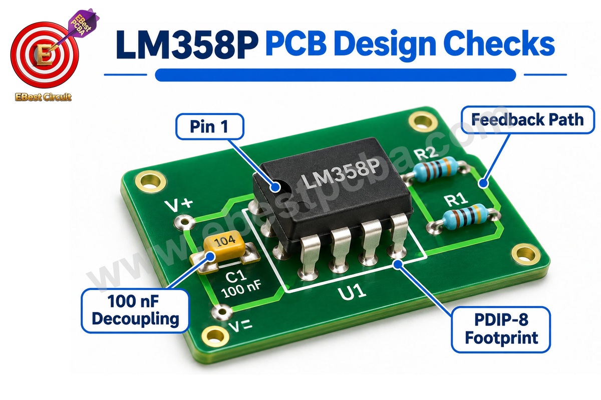
The following considerations are particularly important for analog PCBs.
1. Verify the PDIP-8 Footprint
LM358P uses a through-hole PDIP-8 package.
The footprint should match the manufacturer’s mechanical drawing, including:
-
2.54 mm pin pitch along each row.
-
Correct row spacing.
-
Suitable plated through-hole dimensions.
-
Appropriate pad size and annular ring.
-
Component body clearance.
-
Correct Pin 1 location.
A PDIP-8 footprint cannot be replaced directly with an SOIC-8 footprint because the mounting methods and dimensions differ.
2. Confirm Pin 1 Orientation
The IC package notch or molded marker establishes the orientation reference.
During PCB design and assembly, the schematic, silkscreen, component drawing, and physical package should agree.
Incorrect orientation can result in the power supply being connected to the wrong pins, potentially damaging the IC.
3. Place Decoupling Capacitors Correctly
Supply bypass capacitors should be positioned close to the relevant power connections.
The layout should minimize unnecessary trace length and inductance between the IC, capacitors, and supply return.
A 100 nF ceramic capacitor is a common starting point for local supply decoupling, with additional capacitance selected according to the overall power network.
4. Keep Feedback Paths Short
Feedback components influence amplifier gain and stability.
For example, in a non-inverting amplifier using the first channel, the feedback network connects the output at Pin 1 to the inverting input at Pin 2.
Placing the feedback resistors near the amplifier helps reduce unwanted coupling and parasitic effects.
Sensitive analog inputs should be routed away from high-current switching paths where practical.
5. Check Signal and Load Requirements
Before releasing the PCB, engineers should check whether the chosen supply allows the full expected input signal range.
The output load must also be considered.
For example, a 5 V LM358P circuit should not assume that the amplifier can provide an accurate 5 V output under load.
If the application requires near-rail output operation, a suitable rail-to-rail amplifier may be more appropriate.
6. Confirm the BOM and Approved Part Number
A clear BOM reduces the risk of installing the wrong variant.
| BOM Field | Example |
|---|---|
| Reference | U1 |
| Component | Dual op amp |
| Part Number | LM358P |
| Package | PDIP-8 |
| Quantity | 1 |
| Manufacturer | Texas Instruments |
The BOM should also identify approved substitutes where applicable.
7. Inspect and Test the PCB Assembly
Common LM358P-related problems include incorrect installation, soldering defects, unsuitable supply conditions, and feedback errors.
| Problem | Possible Cause | Recommended Check |
|---|---|---|
| No output | Supply or solder issue | Verify power and joints |
| Output saturation | Invalid signal range | Check input/output limits |
| Wrong gain | Feedback resistor error | Verify resistor values |
| Noise or oscillation | Layout or decoupling | Review routing and supply |
| Incorrect IC | BOM or assembly error | Verify MPN and orientation |
At EBest PCBA, our engineering team can review component footprints, drawing information, and BOM accuracy before manufacturing. Our through-hole assembly and testing capabilities can then support suitable inspection and functional validation for the completed analog PCB.
Why Choose EBest PCBA for LM358P PCB Assembly?
EBest PCBA provides coordinated PCB fabrication, component sourcing, SMT/DIP assembly, inspection, and functional testing for LM358P amplifier boards and other analog electronic products.
Our engineering and manufacturing services help customers address component selection, footprint accuracy, assembly quality, and project requirements through one coordinated team.
-
Free DFM Review: Our engineers review LM358P footprint dimensions, Pin 1 orientation, pad design, component spacing, and manufacturing-related issues before production.
-
No MOQ Support: We support engineering prototypes, low-volume validation, and repeat orders without a fixed minimum order quantity.
-
4 SMT Production Lines: Our 2 JUKI and 2 YAMAHA SMT lines support automated assembly of surface-mount components used alongside LM358P circuits.
-
SMT and DIP Assembly: We support surface-mount components and through-hole packages, including PDIP-8 devices, using suitable soldering processes.
-
Component Sourcing: We coordinate sourcing according to the approved BOM and help review manufacturer part numbers and proposed alternatives.
-
Inspection and Testing: Available capabilities include SPI, AOI, X-Ray inspection where suitable, ICT, and FCT based on the design and project requirements.
-
MES Single-Board Traceability: Our MES system supports production record retrieval and board-level manufacturing traceability.
-
1 Sales Representative + 3 Engineers: Our dedicated communication structure supports engineering feedback, sourcing questions, manufacturing planning, and drawing revisions.
Our manufacturing operations are supported by quality management systems and applicable certifications, including ISO 9001, ISO 13485, IATF 16949, and AS9100D, with certification scope available for supplier qualification review.
If your project involves an LM358P amplifier PCB, sensor signal-conditioning board, voltage-monitoring circuit, or complete PCB assembly, send your Gerber files, BOM, schematic, quantities, and test requirements to sales@ebestpcba.com. Our engineering team can review your manufacturing requirements and provide a tailored quotation and production plan.
Frequently Asked Questions About LM358P Pinout
1. Is LM358P a single or dual operational amplifier?
LM358P is a dual operational amplifier containing 2 independent amplifier channels in an 8-pin package. Amplifier 1 uses Pins 1, 2, and 3, while amplifier 2 uses Pins 5, 6, and 7. Both channels share the positive and negative supply terminals at Pins 8 and 4.
2. What is the function of Pin 4 on the LM358P?
Pin 4 is the negative power supply terminal, identified as V−. In a single-supply circuit, it is commonly connected to ground. In a dual-supply circuit, it may connect to a negative voltage such as −12 V. The supply voltage between Pins 8 and 4 must remain within the device’s specified limits.
3. Can LM358P operate from a 5 V power supply?
Yes. The classic TI LM358P supports operation with a total supply voltage from 3 V to 30 V, so a 5 V supply is within its supported range. Connect Pin 8 to +5 V and Pin 4 to ground. The input common-mode range and output voltage swing still need to be considered.
4. Can the LM358P output reach 5 V with a 5 V supply?
No. The classic LM358P does not provide a rail-to-rail output. Its output requires headroom below the positive supply, depending on the load and operating conditions. Under a 5 V supply, the maximum useful output voltage may be substantially below 5 V. Check the datasheet’s output swing specifications for the intended load.
5. Is LM358P suitable for an audio amplifier?
LM358P can support basic low-frequency audio signal amplification, including simple preamplifier and audio-level sensing circuits. However, its bandwidth, slew rate, noise, distortion, and output-drive characteristics limit its suitability for demanding audio applications. It is not a direct substitute for an audio power amplifier such as LM386.
6. Can LM358B replace LM358P?
An LM358B in a compatible package may serve as an upgraded replacement in many circuits, but the exact orderable part number and package must be verified. LM358B offers improved specifications, including greater bandwidth and a wider supply range. Check input behavior, output loading, electrical limits, and the circuit’s functional requirements before approving substitution.
7. What should I do with an unused LM358P amplifier?
An unused LM358P amplifier should be connected in a stable, defined configuration. A common method is to configure it as a voltage follower by connecting the output to the inverting input and biasing the non-inverting input at a valid reference voltage. The reference must remain within the permitted input common-mode range, and the resulting output must be within its operating limits.
Conclusion
The LM358P pinout provides 2 independent amplifier channels in a standard PDIP-8 configuration, making the device useful for sensor signal conditioning, voltage monitoring, low-frequency amplification, and general analog circuits. Correct pin identification, suitable power supply wiring, feedback design, and PCB footprint verification help engineers achieve reliable performance. When comparing LM358P with LM358N, LM324, or LM386, both pin configuration and electrical functionality must be considered. EBest PCBA supports these projects with Free DFM, No MOQ, component sourcing, SMT/DIP assembly, inspection, and functional testing. Send your project documentation to sales@ebestpcba.com for engineering review and a project-specific PCB assembly quotation.