Key Takeaways
- Electronic components on a PCB include resistors, capacitors, inductors, diodes, transistors, integrated circuits (ICs), connectors, and other devices that perform specific electrical functions.
- A PCB components list with pictures helps engineers and beginners identify common parts by their appearance, package shape, reference designators, and circuit applications.
- PCB reference designators use letters such as R for resistors, C for capacitors, L for inductors, D for diodes, Q for transistors, and U for integrated circuits.
- Active and passive components perform different functions. Active devices support switching, amplification, and signal processing, while passive components provide resistance, capacitance, inductance, and energy transfer.
- PCB component identification involves checking silkscreen markings, package dimensions, polarity, component part numbers, schematics, and the bill of materials (BOM).
- Electronic components are attached to PCBs through surface-mount technology (SMT), through-hole technology (THT), or a combination of both, depending on package design and assembly requirements.
- PCB component selection should consider electrical ratings, footprint compatibility, operating temperature, availability, and approved alternatives before assembly.
- PCB assembly quality relies on appropriate inspection and testing methods, including SPI, AOI, X-Ray inspection, in-circuit testing (ICT), and functional testing (FCT).
Introduction
Electronic components on a PCB are individual electrical devices mounted on a printed circuit board to perform functions such as controlling current, storing electrical energy, processing signals, regulating voltage, and connecting circuits. Common PCB components include resistors, capacitors, diodes, transistors, integrated circuits, and connectors. This guide provides a practical PCB electronic components list, explains their functions, and shows how to identify, select, assemble, and test them.
At EBest PCBA, we support PCB fabrication, electronic component sourcing, SMT and through-hole assembly, inspection, and functional testing. Our manufacturing capabilities include 4 SMT lines, 01005 component assembly, 0.2 mm BGA pitch capability, Free DFM review, and No MOQ support. With 1 sales representative and 3 engineers supporting project communication, we help customers resolve component and assembly requirements from prototypes to repeat production. Send your Gerber files, BOM, and assembly requirements to sales@ebestpcba.com for a project-specific manufacturing review and quotation.
What Electronic Components Are Used in a PCB?
The most common electronic components used in PCBs are resistors, capacitors, inductors, diodes, transistors, integrated circuits, connectors, switches, and protection devices. Each component performs a specific electrical function, while the PCB provides the conductive paths that connect them into a working circuit.
A bare PCB contains copper traces, insulating materials, pads, and vias. Once electronic components are installed and soldered onto the board, it becomes a printed circuit board assembly (PCBA).
PCB electronic components can be grouped according to their functions:
- Passive components: Resistors, capacitors, and inductors manage current, voltage, filtering, and energy storage.
- Semiconductor components: Diodes, transistors, MOSFETs, and integrated circuits perform switching, rectification, amplification, and signal processing.
- Electromechanical components: Connectors, relays, and switches provide electrical connections or mechanical switching.
- Timing and sensing components: Crystals, oscillators, and sensors support timing, measurement, and feedback.
- Protection components: Fuses, TVS diodes, and varistors help protect circuits against excessive current or voltage.
For example, a power supply PCB may contain rectifier diodes, capacitors, inductors, switching MOSFETs, and a controller IC. A sensor PCB may use a sensing element, signal-conditioning circuit, voltage regulator, and communication interface.
The actual combination depends on the circuit’s intended application, operating conditions, and electrical design.
PCB Electronic Components List with Pictures and Functions
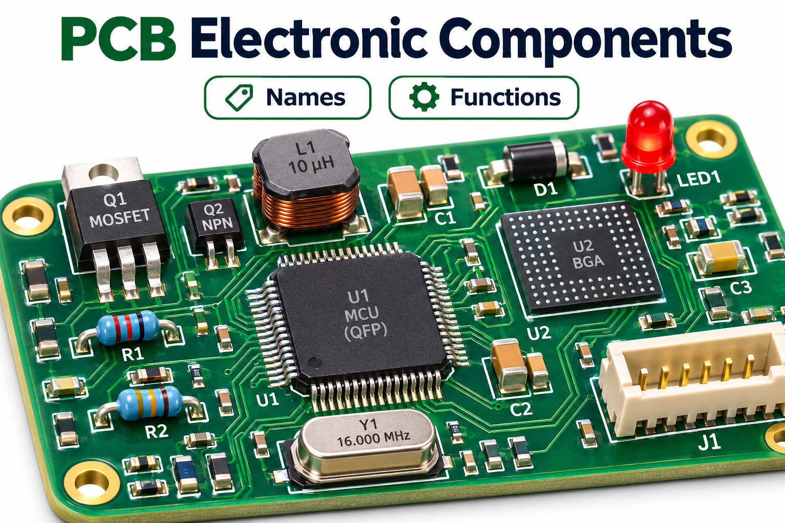
A PCB electronic components list typically includes resistors, capacitors, inductors, diodes, transistors, MOSFETs, ICs, LEDs, connectors, crystals, switches, and fuses. Their names, PCB reference designators, and functions provide a quick way to understand how a circuit board operates.
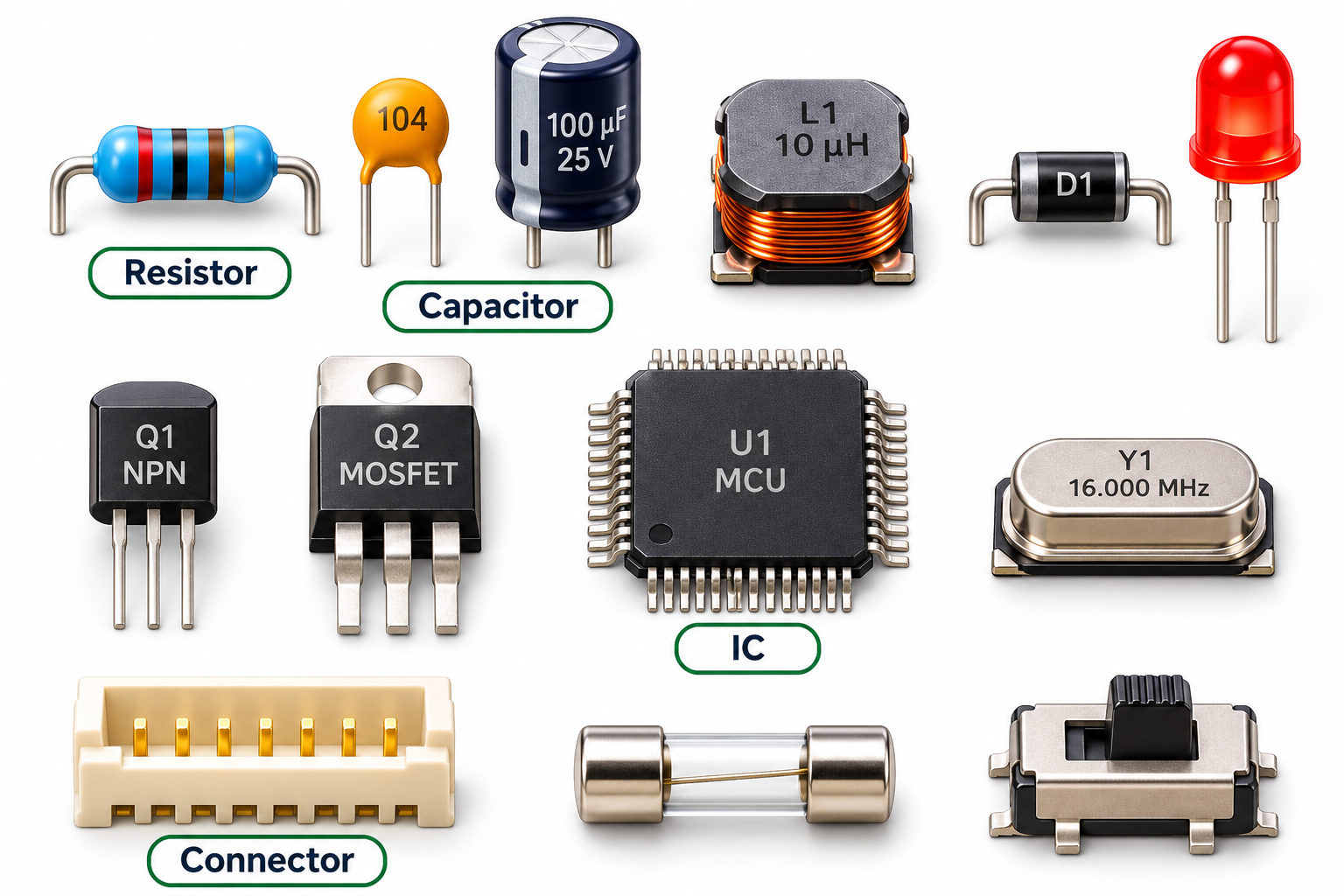
The table below summarizes common PCB board components.
| Electronic Component | PCB Label | Main Function |
|---|---|---|
| Resistor | R | Limits or divides current and voltage |
| Capacitor | C | Stores charge and filters signals |
| Inductor | L | Stores magnetic energy |
| Diode | D | Provides directional conduction |
| LED | D / LED | Emits light |
| Transistor | Q | Switches or amplifies signals |
| MOSFET | Q | Controls electrical switching |
| Integrated Circuit | U | Processes or controls signals |
| Connector | J / P | Connects electrical interfaces |
| Crystal | Y | Provides a frequency reference |
| Switch | SW | Opens or closes a circuit |
| Fuse | F | Protects against overcurrent |
| Ferrite Bead | FB | Suppresses high-frequency noise |
| Relay | K | Switches circuits electrically |
| Sensor | U / other | Measures physical conditions |
Reference designators follow common electronics conventions, although individual CAD libraries and manufacturer standards may use different prefixes.
1. Resistors
Resistors control current, establish voltage levels, and support signal conditioning. They are widely used for voltage dividers, current limiting, pull-up and pull-down networks, and feedback circuits.
Common PCB resistor types include:
- Thick-film SMD resistors: Used in general-purpose electronic circuits.
- Thin-film resistors: Suitable for tighter resistance tolerances and precision applications.
- Current-sense resistors: Used to measure current through a known resistance.
- Resistor networks: Combine multiple resistors into a single package.
Common SMD packages include 0402, 0603, 0805, and 1206 in imperial dimensions. Smaller 0201 and 01005 components support compact PCB layouts but require suitable assembly capability.
A resistor’s selection depends on resistance, tolerance, power rating, temperature coefficient, voltage rating, and package size.
2. Capacitors
Capacitors temporarily store electrical charge and are commonly installed near IC power pins, voltage regulators, and signal-processing circuits.
Typical PCB capacitor types include:
- Multilayer ceramic capacitors (MLCCs): Widely used for decoupling and filtering.
- Aluminum electrolytic capacitors: Often used for bulk energy storage and power smoothing.
- Tantalum capacitors: Used where stable capacitance and compact packaging are important.
- Film capacitors: Used in selected filtering, timing, and power applications.
Important capacitor specifications include capacitance, rated voltage, tolerance, dielectric type, ESR, temperature characteristics, and package dimensions.
For ceramic capacitors, engineers should also consider capacitance reduction under DC bias, particularly when using high-capacitance MLCCs.
3. Inductors
Inductors store energy in a magnetic field and help control current changes. They are commonly found in DC-DC converters, filters, RF circuits, and power management systems.
Common types include:
- Power inductors
- RF inductors
- Shielded inductors
- Common-mode chokes
Important selection parameters include inductance, saturation current, RMS current rating, DC resistance, self-resonant frequency, and physical dimensions.
4. Diodes and LEDs
Diodes are semiconductor components that generally allow current to flow more readily in 1 direction than the other.
Common types include:
- Rectifier diodes: Convert or direct current in power circuits.
- Schottky diodes: Support low forward-voltage applications and fast switching.
- Zener diodes: Provide voltage-reference or voltage-limiting functions.
- TVS diodes: Protect circuits against transient voltage events.
- LEDs: Produce light for indicators, displays, and lighting systems.
Diode orientation is important because the anode and cathode determine how the component functions in a circuit.
5. Transistors and MOSFETs
Transistors are used for switching and amplification. MOSFETs are particularly common in power electronics because their gate-controlled operation supports efficient electrical switching.
Typical applications include motor drivers, power converters, LED drivers, and digital interfaces.
Selection factors include voltage rating, current rating, thermal characteristics, switching performance, and package design.
6. Integrated Circuits (ICs)
Integrated circuits combine multiple electronic functions into a single semiconductor package.
Common IC categories include:
- Microcontrollers and processors
- Operational amplifiers
- Memory devices
- Power management ICs
- Interface controllers
- Communication ICs
- Sensor ICs
Common packages include SOIC, QFN, QFP, BGA, and other surface-mount formats. Package dimensions, pin count, pitch, thermal requirements, and solder-joint accessibility influence PCB design and assembly.
7. Connectors, Crystals, and Protection Devices
Connectors provide power, signal, and communication interfaces. Crystals and oscillators establish timing references, while fuses, varistors, and transient protection devices help protect equipment.
These components are selected according to electrical performance as well as mechanical requirements such as mating cycles, mounting strength, vibration exposure, and available PCB space.
How to Identify Electronic Components on a PCB?
PCB components identification begins with the reference designators printed on the circuit board, followed by component markings, package shape, orientation, and comparison with the BOM or circuit schematic.
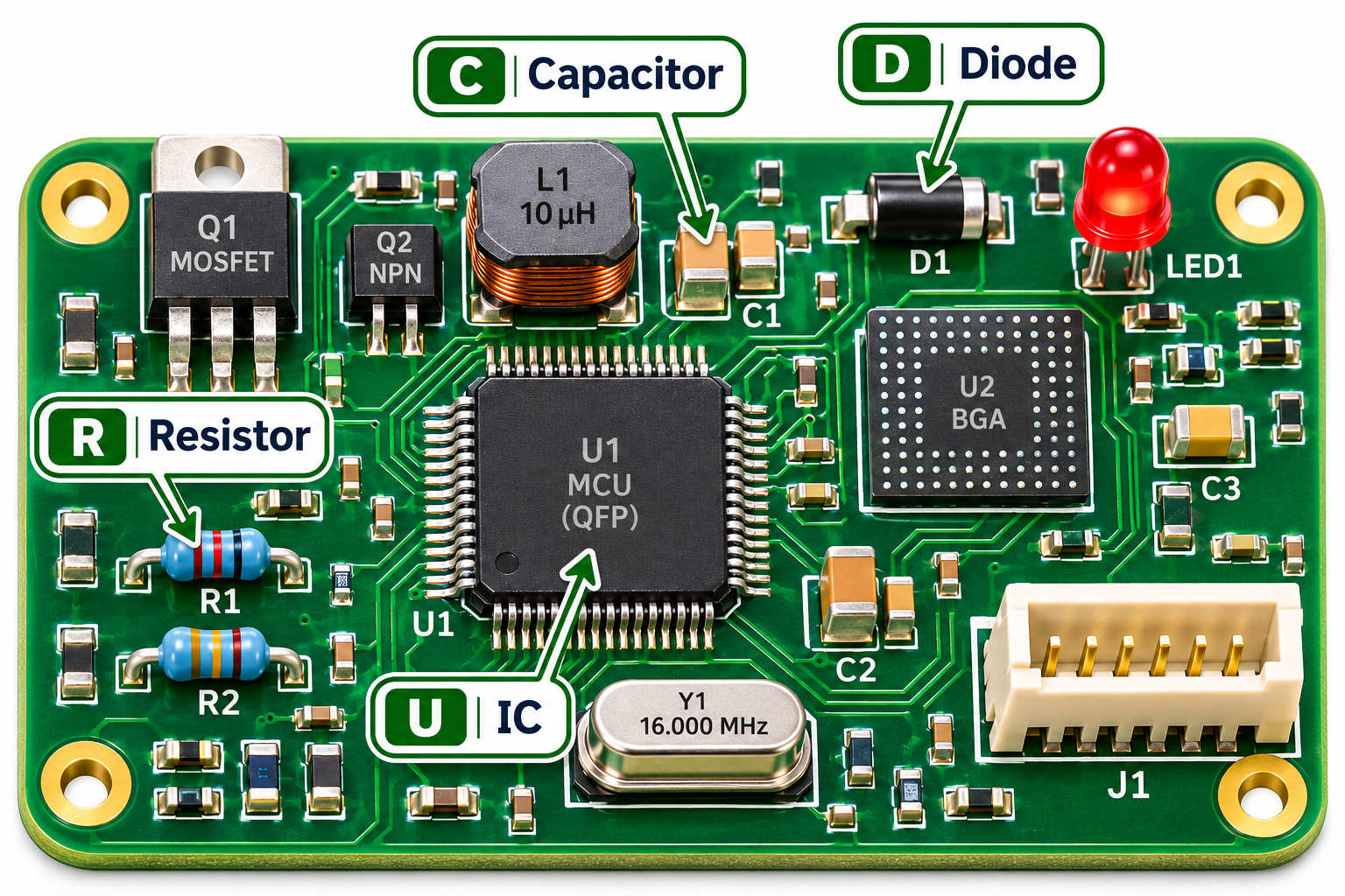
For example, R15 usually indicates a resistor, C8 a capacitor, and U3 an integrated circuit. The letters identify the component category, while the numbers identify individual positions in the design.
1. Read PCB Reference Designators
The following table shows commonly used component markings.
| PCB Marking | Component | Example |
|---|---|---|
| R | Resistor | R12 |
| C | Capacitor | C5 |
| L | Inductor | L3 |
| D | Diode / LED | D4 |
| Q | Transistor / MOSFET | Q2 |
| U | Integrated Circuit | U7 |
| J | Connector | J1 |
| Y | Crystal / Oscillator | Y2 |
| F | Fuse | F1 |
| FB | Ferrite Bead | FB3 |
| SW | Switch | SW1 |
| TP | Test Point | TP6 |
These conventions help connect the physical PCB to its schematic and assembly documentation. Some boards use alternative labels, so the design files remain the authoritative reference.
2. Examine Component Markings
The markings on a component may indicate its resistance, value code, manufacturer, product family, or abbreviated part number.
For example:
- A resistor marked 103 commonly represents 10 kΩ under the 3-digit resistor coding convention.
- A resistor marked 472 commonly represents 4.7 kΩ.
- An IC may carry a short package marking that must be checked against the manufacturer’s marking guide.
- Many small ceramic capacitors have no readable value marking.
A component’s physical appearance rarely provides enough information to confirm its exact electrical specifications.
3. Check Package Shape and Dimensions
Component packages provide additional identification clues.
- Chip resistors and MLCCs often have rectangular ceramic bodies.
- SOIC packages have external leads along 2 sides.
- QFP packages use leads around 4 sides.
- QFN packages use underside or perimeter terminals.
- BGA packages have solder-ball connections beneath the component body.
Package dimensions can help narrow the identification, but similar-looking components may have very different electrical ratings.
4. Identify Polarity and Pin Orientation
Some electronic components require a specific installation direction.
- Diodes: Check the cathode marking against the PCB footprint.
- Polarized capacitors: Verify the package polarity and the PCB polarity marking.
- ICs: Locate the Pin 1 dot, notch, or package orientation indicator.
- LEDs: Identify the anode and cathode using the manufacturer’s documentation.
Polarity markings vary among component families. For example, a stripe on a polarized capacitor does not always identify the same terminal across different capacitor technologies.
5. Cross-Check the BOM and Schematic
The most reliable identification process is to compare the physical component with the approved design documentation.
A useful sequence is:
- Locate the component reference designator.
- Find the corresponding reference in the BOM.
- Check the manufacturer part number and datasheet.
- Verify the package, value, and orientation.
- Compare the actual component with the approved assembly drawing.
For unpowered boards, suitable electrical measurements can provide additional evidence. In-circuit measurements may be affected by parallel circuit paths and surrounding components.
What Is the Difference Between Active and Passive PCB Components?
Active components generally enable amplification, switching, control, or signal processing, while passive components provide resistance, capacitance, inductance, or energy transfer without power gain. Both categories are essential in electronic circuit design.
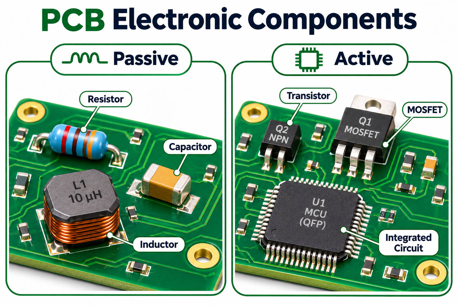
| Feature | Active Components | Passive Components |
|---|---|---|
| Examples | Transistors, ICs | Resistors, capacitors, inductors |
| Main Role | Switching and signal control | Filtering and energy management |
| Gain | Some provide amplification | No power gain |
| Circuit Use | Controllers, amplifiers, drivers | Filters, dividers, matching networks |
Active Components
Active devices are commonly used in circuits that require controlled electrical behavior.
Examples include:
- Microcontrollers executing embedded programs.
- Operational amplifiers conditioning analog signals.
- MOSFETs switching power to motors or LEDs.
- Communication ICs transmitting and receiving data.
Many active circuits require an external supply to operate. However, component classification is based on electrical behavior rather than simply whether a device has a power connection.
Passive Components
Passive components establish electrical conditions and support energy storage or transfer.
Examples include:
- Resistors establishing feedback or bias networks.
- Capacitors filtering supply ripple.
- Inductors storing energy in switching converters.
- Transformer windings transferring electrical energy magnetically.
A practical PCB often combines both categories. For instance, a voltage regulator IC uses capacitors and inductors to maintain a stable supply for other electronic components.
How Do You Choose the Right Electronic Components for a PCB?
Choosing the right PCB electronic components requires checking electrical specifications, package compatibility, operating conditions, supplier availability, and assembly requirements. A component should match both the intended circuit function and the approved PCB design.
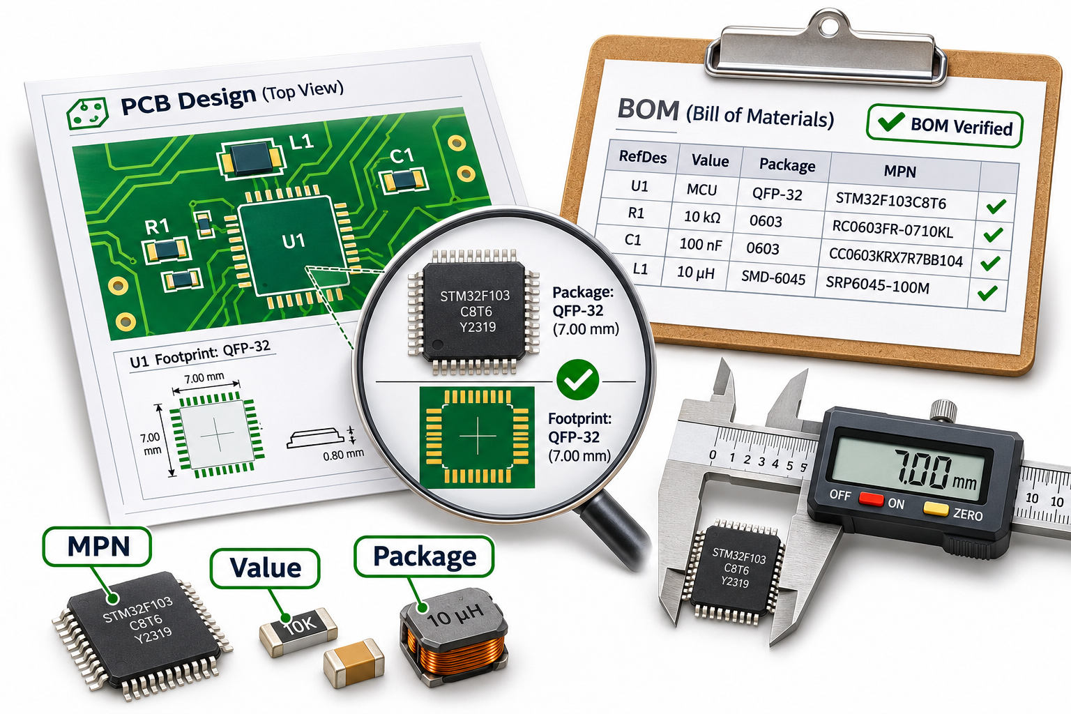
1. Verify Electrical Ratings
Each component must operate within suitable electrical limits.
Important parameters include:
- Resistors: Resistance, tolerance, power dissipation, and temperature coefficient.
- Capacitors: Capacitance, voltage rating, dielectric behavior, and ESR.
- Inductors: Inductance, saturation current, and DC resistance.
- Diodes: Reverse voltage, forward current, and switching characteristics.
- ICs: Supply voltage, interface compatibility, current consumption, and operating temperature.
For example, selecting a capacitor requires more than matching its nominal capacitance. Engineers should consider operating voltage, effective capacitance, ripple requirements, and temperature conditions.
2. Match the Component Footprint
The selected part must correspond to the PCB land pattern.
Before releasing the layout, verify:
- Package dimensions and terminal arrangement.
- Pin numbering and component orientation.
- Pad geometry and solder mask clearances.
- Placement spacing and assembly accessibility.
- Mechanical height and enclosure clearance.
Components with similar package names may use different terminal layouts or recommended footprints.
For fine-pitch devices, pad design, solder paste deposition, placement accuracy, and reflow conditions become especially important.
3. Consider Operating Conditions
Application conditions affect component reliability and useful service life.
Typical factors include operating temperature, humidity, vibration, thermal cycling, and electrical loading.
For power electronics, thermal performance may influence the selection of MOSFETs, inductors, connectors, and high-power resistors. For vibration-sensitive applications, component mass, mounting method, and mechanical support also deserve attention.
4. Review Component Availability and Alternatives
A technically suitable component may create procurement problems if it has limited availability or an extended lead time.
Before approving an alternative, engineers should review:
- Electrical specification equivalence.
- Package and pin compatibility.
- Firmware or functional compatibility where relevant.
- Operating temperature and reliability requirements.
- Approved manufacturer and part-number records.
An alternative with the same nominal value is not automatically interchangeable.
5. Prepare an Accurate BOM
A complete BOM gives the sourcing and assembly teams the information needed to purchase and install the correct parts.
Useful BOM fields include:
| BOM Field | Example |
|---|---|
| Reference | R1, R2 |
| Value | 10 kΩ |
| Package | 0603 |
| Quantity | 2 |
| Manufacturer | Approved supplier |
| MPN | Exact part number |
Additional fields may include approved alternatives, DNI/DNP status, revision information, and sourcing notes.
At EBest PCBA, our engineering and sourcing teams can review BOM information alongside PCB manufacturing and assembly requirements. This helps identify footprint inconsistencies, unclear component specifications, and sourcing questions before production.
How Are Electronic Components Attached to a PCB?
Electronic components are attached to a PCB using surface-mount technology (SMT), through-hole technology (THT), or mixed assembly. Solder joints provide electrical connectivity and mechanical attachment, while the selected assembly method depends on component package design and application requirements.
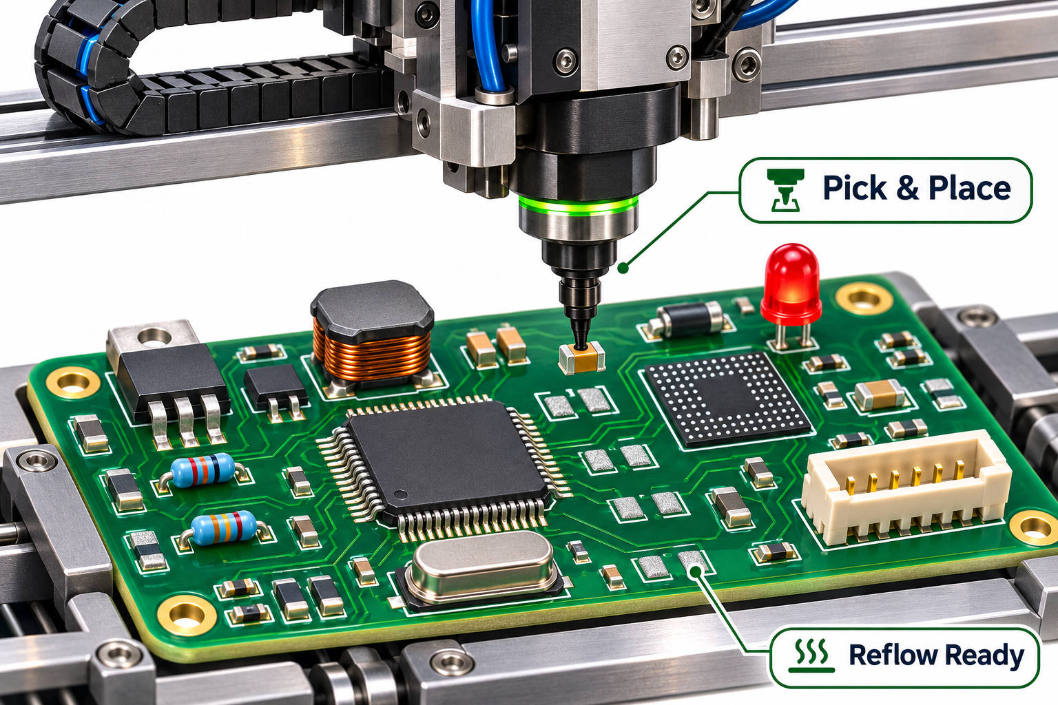
1. Surface-Mount Technology (SMT)
SMT places electronic components directly onto the PCB’s surface pads.
The typical manufacturing sequence includes:
- Solder Paste Printing: Apply solder paste through a stencil onto the specified PCB pads.
- SPI Inspection: Check solder paste deposits for relevant volume, height, area, and alignment defects.
- Component Placement: Use automated pick-and-place equipment to position SMD components.
- Reflow Soldering: Heat the assembly according to a suitable thermal profile to form solder joints.
- AOI Inspection: Examine visible component placement and soldering conditions.
SMT is widely used for compact, high-density electronic products because it supports small packages, automated placement, and double-sided PCB assembly.
At EBest PCBA, our 4 SMT lines include 2 JUKI and 2 YAMAHA lines, supporting automated component placement for different assembly requirements.
2. Through-Hole Technology (THT)
Through-hole components have leads inserted into plated holes in the PCB.
Depending on the design and production volume, these components may be soldered using:
- Wave soldering
- Selective wave soldering
- Manual soldering for suitable operations
THT is frequently used for connectors, transformers, large capacitors, and other components where the package or mechanical requirements favor through-hole attachment.
The finished solder joint should provide suitable electrical connection and mechanical integrity according to the applicable workmanship criteria.
3. Mixed SMT and Through-Hole Assembly
Many PCBA products contain both SMT and THT components.
For example, a control board may use SMT resistors, capacitors, ICs, and MOSFETs alongside through-hole power connectors and relays.
A typical mixed-technology workflow may involve:
- SMT assembly and reflow soldering.
- Through-hole component insertion.
- Wave, selective, or other approved soldering processes.
- Visual inspection and electrical testing.
The exact process order depends on the PCB layout, component temperature limits, and manufacturing requirements.
4. Fine-Pitch Electronic Component Assembly
Fine-pitch packages require controlled solder paste printing, placement accuracy, and soldering conditions.
EBest PCBA supports 01005 component assembly and BGA packages with pitches down to 0.2 mm, subject to project-specific design and manufacturing review.
Our assembly process can incorporate:
- Fine-pitch placement capability.
- Nitrogen reflow soldering.
- Solder paste inspection.
- Automated optical inspection.
- X-Ray inspection for suitable hidden solder joints.
For complex packages, early DFM review helps establish suitable footprint, stencil, clearance, and inspection requirements.
How Are PCB Electronic Components Inspected and Tested?
PCB electronic components are inspected and tested using a combination of solder paste inspection, optical inspection, X-Ray inspection, electrical testing, and functional testing. These methods detect different defect categories and provide complementary evidence of assembly quality.
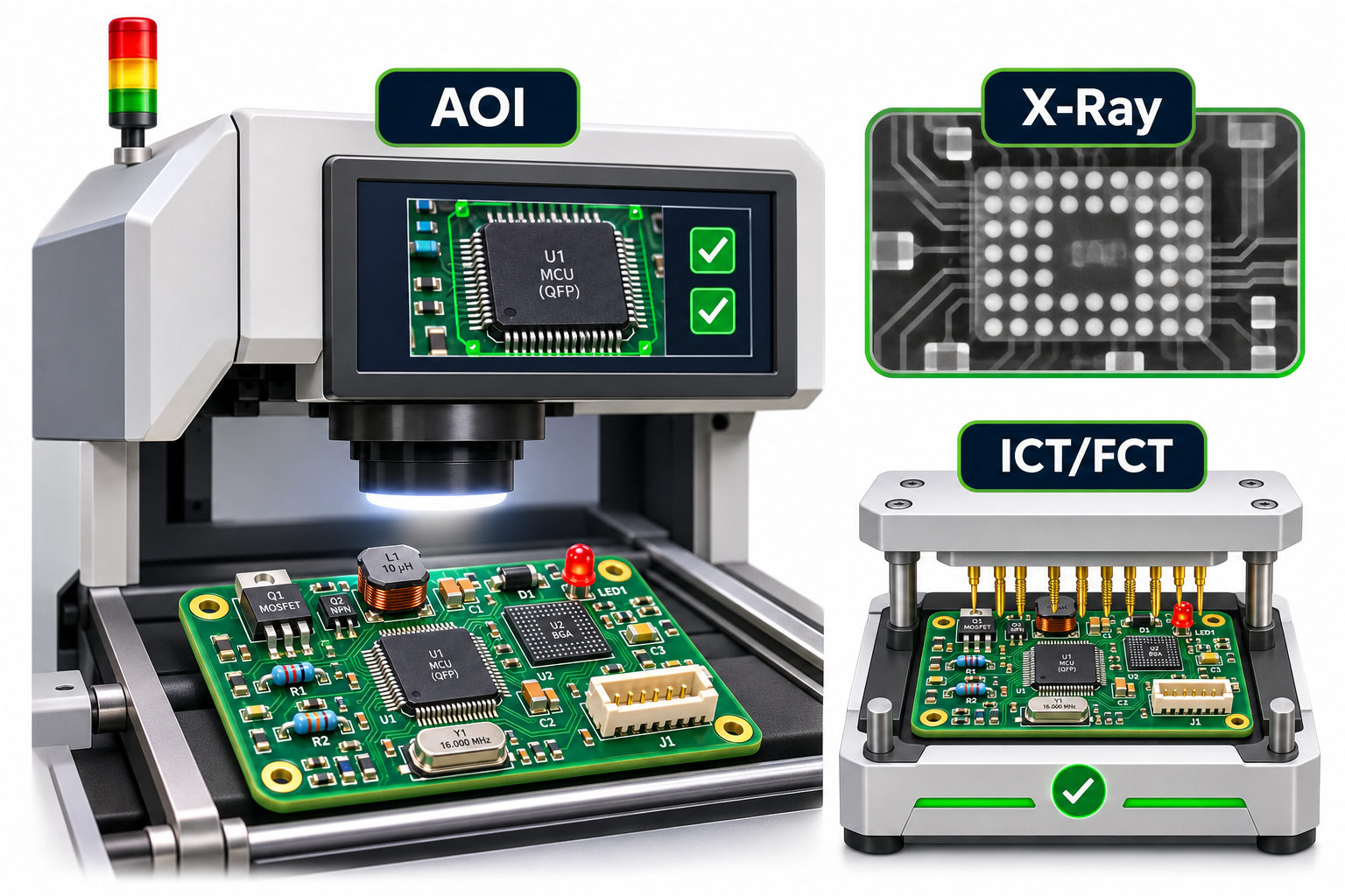
No single inspection method can verify every component characteristic or electrical function.
1. Solder Paste Inspection (SPI)
SPI examines solder paste deposits before component placement.
It helps identify:
- Insufficient solder paste.
- Excessive solder paste.
- Misaligned deposits.
- Height and volume inconsistencies.
Controlling solder paste deposition is particularly important for fine-pitch ICs, small passive components, and dense PCB layouts.
2. Automated Optical Inspection (AOI)
AOI uses optical imaging to examine visible assembly features.
Depending on the inspection system and programming, it can detect:
- Missing components.
- Component misalignment.
- Some polarity and orientation errors.
- Visible solder bridges.
- Certain solder-joint defects.
AOI is useful for identifying assembly defects early, although it cannot directly verify electrical performance or fully inspect hidden solder joints.
3. X-Ray Inspection
X-Ray inspection examines internal or visually inaccessible assembly features.
It is especially useful for packages such as BGA and selected QFN devices, where solder connections are concealed beneath the component.
Depending on the equipment and analysis method, X-Ray inspection can help assess:
- Hidden solder bridges.
- Solder voids.
- Ball alignment.
- Certain open-joint indications.
- Internal solder-joint conditions.
X-Ray images provide structural information rather than direct confirmation of electrical functionality.
4. In-Circuit Testing (ICT)
ICT checks selected electrical characteristics and connections within an assembled board.
Depending on the test strategy and board accessibility, ICT may identify:
- Shorts and opens.
- Incorrect component values.
- Certain missing or defective components.
- Specific assembly-related electrical faults.
ICT coverage depends on the test equipment, available test points, fixture design, and circuit architecture.
5. Functional Circuit Testing (FCT)
FCT checks whether the assembled PCB performs its intended electrical functions under defined test conditions.
Typical test items may include:
- Power-up behavior.
- Supply voltage and current.
- Input and output responses.
- Communication interfaces.
- Signal generation or measurement.
- Firmware-related functions.
The actual test scope must be established using the product specifications and approved acceptance criteria.
The table below summarizes each method.
| Method | Primary Inspection Target | Typical Stage |
|---|---|---|
| SPI | Solder paste deposits | Before placement |
| AOI | Visible assembly defects | After reflow |
| X-Ray | Hidden solder joints | After soldering |
| ICT | Selected electrical faults | After assembly |
| FCT | Circuit functionality | Final verification |
At EBest PCBA, these inspection and testing capabilities can be incorporated according to each project’s requirements. Our MES system also supports single-board traceability, helping manufacturing and quality teams retrieve production information associated with individual boards.
What PCB Component Problems Can Affect Assembly Quality?
Common PCB component problems include incorrect polarity, wrong component values, package mismatches, missing parts, placement errors, and soldering defects. Many of these issues can be reduced through accurate design data, component verification, DFM review, and controlled assembly processes.
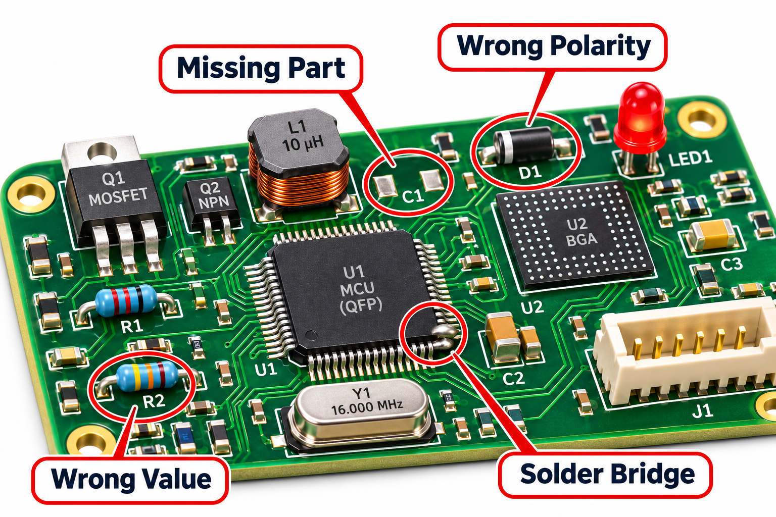
The following table summarizes typical problems and preventive actions.
| Problem | Main Cause | Prevention |
|---|---|---|
| Wrong polarity | Incorrect orientation | Verify polarity and Pin 1 |
| Wrong component | BOM or loading error | Check MPN and feeder setup |
| Footprint mismatch | Incorrect land pattern | Review package drawings |
| Missing component | Placement or kitting error | Verify placement and inspect |
| Solder bridge | Paste or reflow issue | Optimize stencil and profile |
| Insufficient solder | Low paste deposition | Monitor SPI results |
| Tombstoning | Uneven wetting forces | Review pad and reflow conditions |
| Open BGA joint | Joint formation issue | Review process and X-Ray |
| Component damage | Handling or thermal stress | Control handling and reflow |
Incorrect Component Orientation
Polarized capacitors, diodes, LEDs, and many ICs must be installed in the correct orientation.
A mismatch between the schematic, footprint, silkscreen, and placement file can cause assembly errors.
A practical prevention method is to verify Pin 1 indicators, cathode markings, and component orientation during DFM and first-article checks.
Wrong Component Values or Part Numbers
Components with similar physical dimensions may have very different electrical ratings.
For example, 2 resistors in the same 0603 package can have completely different resistance values. Ceramic capacitors may also share package dimensions while differing in capacitance, rated voltage, and dielectric characteristics.
Checking the approved BOM and manufacturer part number is essential before production.
PCB Footprint and Package Mismatch
A component may appear suitable in the schematic but fail to match the PCB footprint.
Common causes include incorrect pad spacing, pin mapping, component orientation, or package dimensions.
DFM review can identify these concerns before the board reaches assembly.
Soldering Defects
Solder bridges, insufficient solder, tombstoning, and incomplete solder joints may result from several interacting factors, including stencil design, solder paste behavior, pad geometry, placement, and reflow conditions.
The appropriate corrective action depends on the defect mechanism. For example, tombstoning may require reviewing pad symmetry, solder paste balance, component placement, and heating behavior.
Component Sourcing and Substitution Errors
Substituting a component without proper review can create electrical or manufacturing problems.
Even when 2 parts share a nominal value, differences in pinout, voltage rating, thermal behavior, tolerance, and package construction may affect the finished PCB.
For this reason, EBest PCBA encourages component and BOM review before assembly, particularly when a project involves alternative parts, fine-pitch packages, or critical electrical requirements.
Why Choose EBest PCBA for Electronic Component Sourcing and PCB Assembly?
EBest PCBA provides coordinated electronic component sourcing, PCB fabrication, SMT/DIP assembly, inspection, testing, and box build services, helping customers manage component requirements and manufacturing activities through a single project team.
Whether you are preparing an engineering prototype or planning repeat production, our services are designed to address practical manufacturing and purchasing requirements.
- Free DFM Review: Our engineers review PCB design files and manufacturing requirements, helping identify footprint, placement, assembly, and process concerns before production.
- No MOQ Support: We support engineering prototypes, low-volume assembly, and subsequent production orders without a fixed minimum order quantity.
- 4 SMT Production Lines: Our 2 JUKI and 2 YAMAHA lines provide automated assembly capacity for a wide range of electronic products.
- Fine-Pitch Assembly: Capabilities include 01005 SMD components and BGA pitches down to 0.2 mm, subject to appropriate design and process review.
- Component Sourcing Support: We coordinate component purchasing, BOM checks, and alternative-part discussions with the customer’s approved requirements.
- Inspection and Testing: Available processes include SPI, AOI, X-Ray, ICT, and FCT, selected according to the board design and test coverage requirements.
- MES Single-Board Traceability: Production records support board-level traceability and efficient manufacturing information retrieval.
- 1 Sales Representative + 3 Engineers: A dedicated communication structure helps coordinate engineering feedback, sourcing questions, manufacturing requirements, and project revisions.
Our manufacturing services are supported by quality management certifications, including ISO 9001, ISO 13485, IATF 16949, and AS9100D, with the applicable certification scope available for supplier qualification review.
If your project requires PCB manufacturing, electronic component sourcing, SMT assembly, through-hole soldering, or complete PCBA testing, send your Gerber files, BOM, pick-and-place data, quantities, and testing requirements to sales@ebestpcba.com. Our engineering team can review your specifications and provide a project-specific quotation and manufacturing plan.
Frequently Asked Questions About PCB Electronic Components
1. What are the most common electronic components on a PCB?
The most common PCB components are resistors, capacitors, inductors, diodes, transistors, integrated circuits, and connectors. Resistors control current and voltage, capacitors support filtering, inductors store magnetic energy, and semiconductor devices perform switching, signal processing, and control functions. The actual component selection depends on the circuit application.
2. What do R, C, L, D, Q, and U mean on a PCB?
R identifies a resistor, C a capacitor, L an inductor, D a diode or LED, Q a transistor, and U an integrated circuit. These reference designators are commonly printed on the PCB silkscreen and associated with the schematic and BOM. The numbers following each letter identify individual component positions.
3. How can I identify an unknown SMD component?
Start by checking the PCB reference designator, component package, visible markings, and terminal arrangement. Compare the findings with the schematic, BOM, and manufacturer datasheet. Small SMD components may have no markings, while IC top markings may be abbreviated. Electrical measurements can help when performed under appropriate conditions.
4. What is the difference between SMD and through-hole components?
SMD components are mounted directly onto surface pads, while through-hole components have leads inserted into PCB holes. SMD supports compact layouts and automated assembly. Through-hole packages are often selected for particular connectors, large components, or mechanical requirements. Many PCBs combine both technologies.
5. How do I identify positive and negative terminals on PCB components?
Check the component datasheet, package markings, and PCB polarity indicators. Diodes usually identify the cathode, while polarized capacitors use markings that depend on their construction. Integrated circuits use Pin 1 indicators rather than simple positive and negative markings. Always verify the relevant manufacturer’s orientation convention before assembly.
6. Can different electronic components use the same PCB footprint?
Yes, different components can share a PCB footprint if their package dimensions, terminal configuration, and land-pattern requirements are compatible. However, identical footprints do not guarantee electrical interchangeability. Voltage, current, pinout, tolerance, thermal performance, and circuit function must also be checked before approving a substitute.
7. What files are needed for PCB component sourcing and assembly?
A typical PCB assembly package includes Gerber files, drill files, a BOM with manufacturer part numbers, pick-and-place data, and assembly drawings. Additional files may include schematics, firmware, approved alternatives, testing procedures, and quality requirements. EBest PCBA can review these documents to establish sourcing, manufacturing, inspection, and delivery requirements before quotation.
Conclusion
Understanding PCB electronic components helps engineers identify parts, verify electrical specifications, select compatible packages, and prepare reliable assembly documentation. A clear component list, accurate reference designators, and an approved BOM make the transition from circuit design to manufacturing more manageable. EBest PCBA supports this process through electronic component sourcing, Free DFM, No MOQ, 4 SMT lines, fine-pitch assembly, testing, and MES traceability. For your next PCB assembly project, share your design files and requirements with sales@ebestpcba.com to receive engineering feedback and a tailored quotation.