AOI vs X-Ray inspection for PCB assembly comes down to one important difference: AOI detects visible component and soldering defects, while X-Ray reveals hidden solder connections beneath packages such as BGA and QFN. AOI is well suited to routine SMT inspection, whereas X-Ray provides additional coverage for concealed joints, solder voids, and internal bridging. Using the right method helps manufacturers find assembly defects before they reach final testing or customers.
This guide compares AOI and X-Ray inspection, explains which defects each method can detect, and shows engineers and purchasing teams how to choose an effective inspection plan.
At EBest PCBA, we combine PCB manufacturing, component sourcing, SMT assembly, AOI, X-Ray inspection, and electrical testing in one coordinated service. Our four SMT lines, fine-pitch assembly capabilities, and MES traceability help customers manage PCB assembly quality from prototypes to repeat production.
What Is the Difference Between AOI and X-Ray Inspection?
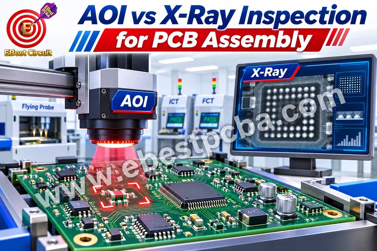
AOI uses cameras and controlled lighting to inspect visible PCB assembly features. X-Ray uses radiographic imaging to examine solder connections and internal structures that optical cameras cannot directly see.
| Comparison | AOI Inspection | X-Ray Inspection |
|---|---|---|
| Technology | Optical cameras | X-ray imaging |
| Main focus | Visible assembly defects | Hidden solder defects |
| Component polarity | Strong coverage | Limited |
| Visible solder joints | Strong coverage | Selective |
| BGA solder balls | Hidden from view | Inspectable |
| Internal solder voids | Not directly visible | Inspectable |
| Typical use | Routine SMT inspection | Targeted hidden-joint inspection |
| Inspection cost | Generally lower | Generally higher |
AOI is generally more practical for inspecting component placement and exposed solder joints across production batches. X-Ray becomes valuable when the package geometry prevents direct optical inspection.
For example, AOI can verify that a BGA is present and positioned correctly. X-Ray can examine the solder-ball pattern beneath that BGA.
Neither method independently confirms full circuit functionality. Electrical and functional testing provide different evidence.
How Does AOI Inspection Work in SMT Assembly?
Automated Optical Inspection (AOI) uses high-resolution cameras, controlled illumination, and image-processing software to identify visible manufacturing defects.
During inspection, an AOI inspection system captures PCB images and compares selected features against programmed references and acceptance limits.
A typical AOI inspection process includes:
- Image capture: Cameras record components and exposed solder joints.
- Feature comparison: Software evaluates position, orientation, markings, and visible solder characteristics.
- Defect identification: Features outside programmed limits are flagged.
- Operator verification: Suspected defects are reviewed before repair or acceptance.
Common PCB Assembly Defects Detected by AOI
| Defect | Typical AOI Finding |
|---|---|
| Missing component | Empty footprint |
| Wrong polarity | Reversed orientation |
| Component offset | Position mismatch |
| Tombstoning | Lifted chip component |
| Solder bridge | Connected visible leads |
| Lifted lead | Lead-height abnormality |
| Insufficient solder | Irregular visible fillet |
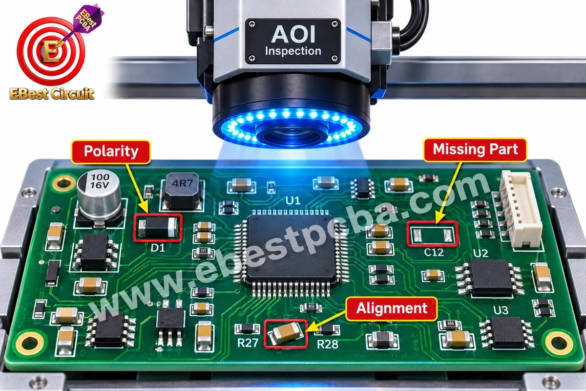
AOI works particularly well with components whose bodies, leads, and solder joints remain optically accessible. These include chip resistors, capacitors, SOIC packages, QFP devices, and many connectors.
2D AOI vs 3D AOI
- 2D AOI: Examines surface images, component markings, and visible geometry.
- 3D AOI: Adds height and surface-profile measurements, improving assessment of certain lifted components, leads, and solder features.
AOI inspection equipment depends on optical visibility, including systems using 3D AOI technology. Both technologies depend on optical visibility. Even a 3D AOI system cannot inspect solder balls concealed beneath a BGA package.
How Does X-Ray Inspection Detect Hidden Solder Defects?
X-Ray inspection examines solder structures by measuring how X-rays pass through different materials. Because solder and surrounding materials attenuate X-rays differently, concealed connections can appear in radiographic images.
Common X-Ray inspection applications include:
- BGA: Solder-ball arrangement, bridging, and voiding.
- QFN: Exposed-pad solder coverage and thermal-pad voids.
- LGA: Concealed land connections.
- CSP: Fine-pitch solder-joint structures.
- Through-hole soldering: Selected hole-fill and internal solder conditions.
2D, 2.5D, and 3D X-Ray Inspection
| Method | Imaging Capability | Typical Use |
|---|---|---|
| 2D X-Ray | Single projection | Solder bridges, voids |
| 2.5D X-Ray | Angled views | Overlapping structures |
| 3D X-Ray / CT | Reconstructed internal slices | Complex failure analysis |

2D X-Ray is useful for many routine examinations, particularly when solder joints are clearly separated in the image. Angled inspection can improve visibility where package features overlap. More advanced 3D systems can reconstruct internal structures for detailed examination.
Imaging capability varies by equipment. A conventional X-Ray system should not automatically be described as 3D AXI or computed tomography.
Automated X-Ray Inspection (AXI) refers to systems using automated image acquisition and analysis. X-Ray inspection may also be performed manually or with operator-assisted equipment.
For BGA assemblies, X-Ray can reveal many solder anomalies that AOI cannot access, although some incomplete or cracked connections remain difficult to diagnose from radiographic images alone.
Which PCB Assembly Defects Can AOI and X-Ray Detect?
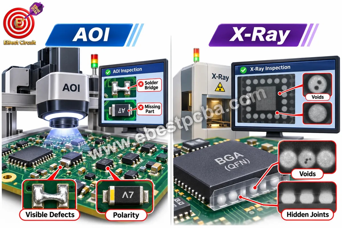
AOI is generally better for visible component and soldering faults, while X-Ray is better for concealed joints and internal solder conditions.
| Assembly Defect | AOI | X-Ray |
|---|---|---|
| Missing component | Strong | Possible |
| Wrong polarity | Strong | Limited |
| Component misalignment | Strong | Possible |
| Tombstoning | Strong | Possible |
| Visible solder bridge | Strong | Detectable |
| Hidden solder bridge | No direct view | Strong |
| BGA solder void | No direct view | Strong |
| QFN thermal-pad void | No direct view | Strong |
| Hidden solder open | No direct view | Conditional |
| Internal solder crack | No direct view | Conditional |
Coverage depends on component geometry, inspection equipment, viewing angles, and programmed criteria.
Where AOI Has an Advantage
AOI is particularly effective at detecting assembly errors associated with component placement and visible soldering. For example, an incorrectly oriented polarized capacitor may be identified through its visible markings and footprint position. AOI can also identify a tombstoned chip resistor because one end is visibly raised from the PCB.
Where X-Ray Has an Advantage
X-Ray becomes useful when solder joints are hidden beneath a package. A BGA may appear correctly placed from above while an X-Ray image reveals a solder bridge between adjacent balls.
X-Ray can also show voiding inside solder joints. Whether a particular void is acceptable depends on package type, joint location, applicable criteria, and customer requirements. Head-in-pillow joints or partial opens may require more advanced views or supplementary analysis.
Why Do BGA and QFN Assemblies Need X-Ray Inspection?
BGA and QFN packages contain solder connections underneath the component body. These connections are difficult or impossible to evaluate completely through ordinary surface inspection.
BGA X-Ray Inspection
BGA packages use an array of solder balls beneath the component. X-Ray inspection can help engineers identify:
- Missing or abnormal solder balls.
- Solder bridging between adjacent connections.
- Significant solder voiding.
- Irregular ball geometry.
- Certain package alignment problems.
QFN X-Ray Inspection
QFN packages commonly use bottom-side solder terminals and an exposed thermal pad. X-Ray can help evaluate:
- Solder voids beneath the exposed pad.
- Solder distribution across the thermal pad.
- Hidden bridging between terminals.
- Abnormal solder coverage.
Thermal-pad voiding is particularly relevant to power devices because the soldered interface can influence heat transfer. Acceptable voiding limits should come from the component manufacturer’s recommendations, applicable standards, and the approved assembly specification rather than one universal percentage.
Can AOI Replace X-Ray Inspection in PCB Assembly?
AOI can provide sufficient visual inspection coverage for many conventional PCB assemblies, but it cannot replace X-Ray when critical solder connections are hidden beneath components.
AOI may be sufficient when:
- Most solder joints are externally visible.
- The assembly primarily uses resistors, capacitors, SOIC, and QFP packages.
- Inspection requirements focus on component placement, polarity, and visible solder defects.
- Additional X-Ray coverage is not required by the product specification.
X-Ray should be considered when:
- The assembly contains BGA, LGA, CSP, or similar bottom-terminated packages.
- QFN thermal-pad soldering requires evaluation.
- Hidden solder bridges or voids are significant risks.
- Customer specifications require radiographic inspection.
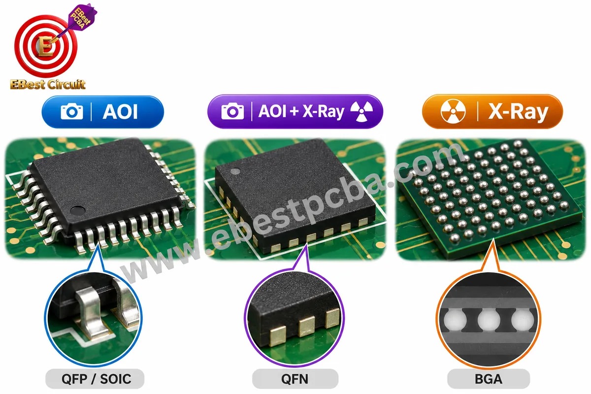
Using both is often the better approach for mixed-component PCBAs. AOI handles visible assembly features, while X-Ray covers selected solder structures that optical inspection cannot reach.
For example, a controller board containing hundreds of small passives, several QFP components, and a fine-pitch BGA would benefit from AOI inspection across the assembly and X-Ray examination of the BGA connections.
When Should AOI and X-Ray Be Performed During SMT Assembly?
AOI is commonly performed after reflow soldering, while X-Ray inspection is typically scheduled after reflow for selected components, production samples, or defined inspection requirements.
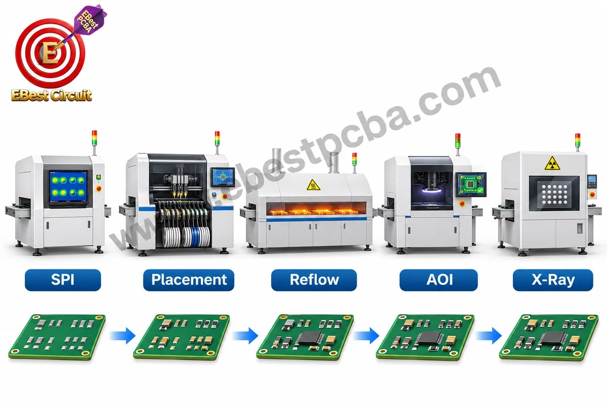
After solder paste printing
SPI can measure paste volume, height, area, and position before component placement. This helps identify printing defects early.
After component placement
Pre-reflow AOI, where implemented, can verify component presence, position, and orientation before soldering.
After reflow soldering
Post-reflow AOI checks visible component and soldering conditions. X-Ray can then examine selected hidden joints, such as BGA solder balls and QFN thermal pads.
Before product release
Where required, ICT and functional testing verify electrical connections and defined circuit functions.
How Do AOI and X-Ray Inspection Affect PCB Assembly Cost?
AOI generally offers lower inspection cost per board for routine visible-defect screening, while X-Ray inspection usually adds equipment, programming, imaging, and review costs.
| Cost Factor | AOI | X-Ray |
|---|---|---|
| Equipment investment | Generally lower | Generally higher |
| Inspection speed | Usually faster | Depends on scan scope |
| Programming effort | Component library and rules | Imaging and defect rules |
| Main cost driver | Coverage and false calls | Scan count and analysis |
| Suitable production use | Broad routine inspection | Targeted or defined coverage |
Three ways to control inspection costs:
- Prioritize hidden joints: Focus X-Ray inspection on BGA, QFN, and similar packages.
- Define inspection frequency: Specify first articles, samples, every board, or particular components.
- Agree on acceptance limits: Establish voiding and defect criteria before production.
A prototype run may justify additional inspection to identify process weaknesses. Once the design and assembly process are stable, inspection frequency can be reviewed against actual defect history and customer requirements.
What PCB Assembly Inspection Standards Should Engineers Follow?
PCB assembly inspection should follow applicable workmanship standards, component manufacturers’ recommendations, and customer-approved acceptance criteria.
| Standard | Application |
|---|---|
| IPC-A-610 | Electronic assembly acceptability |
| IPC J-STD-001 | Soldered assembly requirements |
| IPC-7095 | BGA design and assembly guidance |
| IPC-7351 | Surface-mount land pattern design |
| IPC-TM-650 | Relevant test methods |
IPC-A-610 establishes visual acceptability requirements for electronic assemblies. J-STD-001 addresses requirements for soldered electrical and electronic assemblies. The applicable revision and acceptance class should be agreed upon during project qualification.
Before production, agree on:
- Acceptance class: Applicable IPC classification.
- Standard revision: Specific revision required.
- Component criteria: Package-specific soldering limits.
- X-Ray scope: Selected packages, frequency, and inspection views.
- Defect disposition: Acceptance, repair, rejection, and reinspection.
- Documentation: Required images and records.
BGA X ray inspection criteria should define package-specific acceptance limits and the required evidence. For BGA inspection, the manufacturer should know which packages require examination and whether void measurements or retained images are expected.
Why Choose EBest PCBA for AOI and X-Ray Inspection?
EBest PCBA combines SMT manufacturing, AOI, X-Ray inspection, and electrical testing to help customers identify assembly defects, reduce rework, and maintain consistent production quality. Our service coordinates DFM, PCB fabrication, component sourcing, assembly, inspection, and testing within one manufacturing project.
Our PCB Assembly and Inspection Capabilities
| Capability | EBest PCBA |
|---|---|
| SMT Production | 4 Lines: 2 JUKI + 2 YAMAHA |
| Small Components | Down to 01005 |
| Fine-Pitch BGA | Down to 0.2 mm |
| Solder Paste Inspection | 3D SPI |
| Optical Inspection | AOI |
| Hidden Joint Inspection | X-Ray / AXI |
| Electrical Testing | ICT |
| Functional Testing | Project-Specific FCT |
| Production Traceability | MES Single-Board Tracking |
| Engineering Review | Free DFM |
| Minimum Order | No MOQ |
How EBest PCBA Helps Your Project
- Fine-Pitch Assembly and Inspection: SMT capability for 01005 components and BGA down to 0.2 mm pitch, with inspection planning for dense assemblies.
- Defect Detection at Different Stages: SPI, AOI, and X-Ray help identify printing, placement, visible soldering, and hidden-joint defects.
- Dedicated Engineering Support: One sales representative and three engineers coordinate design, BOM, assembly, and inspection questions.
- Electrical and Functional Verification: ICT and FCT support project-specific testing alongside inspection.
- MES Traceability: Single-board tracking supports record retrieval and quality investigations.
- Flexible Order Quantities: No MOQ and free DFM review support prototypes and repeat production.
Our quality management certifications include ISO 9001, ISO 13485, IATF 16949, and AS9100D, supporting customer supplier qualification across industries.
Need PCB assembly with AOI and X-Ray inspection? Send your Gerber files, BOM, quantities, and inspection requirements to sales@ebestpcba.com for a free DFM review, quotation, and delivery schedule confirmation.
FAQs about AOI vs X-Ray Inspection
1. Is AOI or X-Ray inspection better for PCB assembly?
AOI is better for visible component and soldering defects, while X-Ray is better for hidden solder connections. Assemblies with exposed leads and BGA or QFN packages often benefit from both.
2. Can AOI detect BGA solder defects?
AOI can check visible BGA placement and orientation, but it cannot directly inspect the solder balls beneath the package. X-Ray is more suitable for hidden BGA solder structures.
3. Does every PCB assembly require X-Ray inspection?
No. PCBAs with accessible solder joints can often be inspected using AOI and other appropriate checks. X-Ray is especially valuable for hidden-joint packages and specific reliability requirements.
4. Can X-Ray inspection detect head-in-pillow defects?
Some head-in-pillow defects can be identified using angled or advanced X-Ray inspection. Certain defects remain difficult to distinguish and may require additional electrical testing or analysis.
5. What is the difference between AOI and AXI?
AOI uses optical cameras to inspect visible features. AXI uses radiographic imaging and automated analysis to examine selected internal or hidden structures.
6. Does a PCBA still need ICT or FCT after passing AOI and X-Ray?
Electrical or functional testing may still be necessary. AOI and X-Ray inspect physical assembly conditions; ICT checks selected electrical characteristics, and FCT checks defined circuit functions.
7. How should X-Ray inspection requirements be specified for BGA assemblies?
Specify packages, inspection frequency, acceptance criteria, and any image or measurement records before manufacturing.
Conclusion
AOI vs X-Ray inspection is about defect coverage rather than which technology is universally better. AOI identifies visible placement and soldering faults, while X-Ray reveals concealed solder structures beneath BGA, QFN, and other bottom-terminated packages. Selecting the right combination improves inspection coverage and helps reduce costly assembly defects.
At EBest PCBA, four SMT lines, SPI, AOI, X-Ray, ICT, FCT, and MES traceability support PCB assembly quality from prototypes to production. Send your PCB files, BOM, and inspection requirements to sales@ebestpcba.com for a project-specific manufacturing review and quotation.