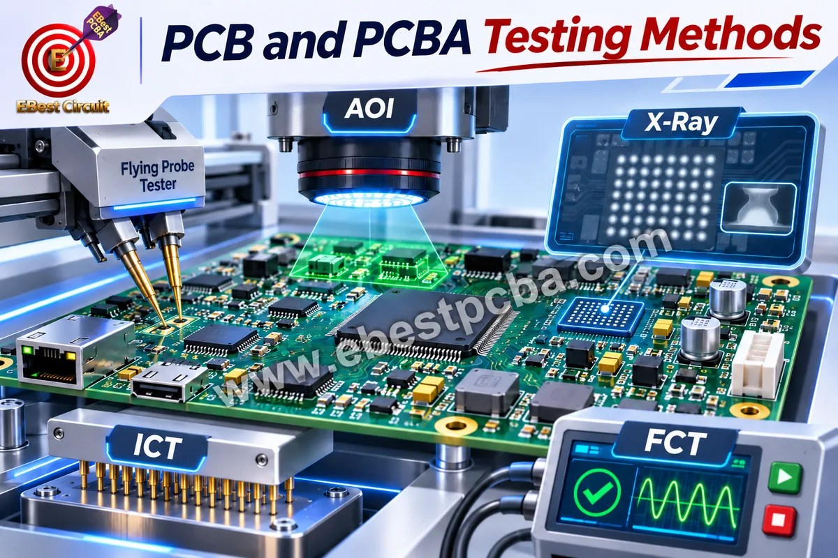
PCB and PCBA testing methods verify electrical connections, soldering quality, component placement, and circuit performance at different manufacturing stages. A bare PCB can pass continuity testing but still develop interconnect problems under thermal stress. Similarly, an assembled board may look perfect under optical inspection yet fail during operation. Choosing the right tests helps manufacturers detect defects earlier, reduce rework, and deliver more consistent products.
This guide compares common PCB and PCBA tests, explains what each method proves, and helps engineers and buyers select suitable inspection methods for prototypes and production.
At EBest PCBA, we provide PCB fabrication, component sourcing, SMT assembly, inspection, and functional testing. With four SMT lines, SPI, AOI, X-ray inspection, ICT, FCT, and MES traceability, we support product quality from initial prototypes to repeat production.
Key Takeaways
- Bare-board electrical tests verify specified connectivity; they do not validate the completed assembly.
- SPI, AOI and X-ray inspect different physical features; ICT and functional testing add selected electrical checks.
- Choose coverage around failure risk, test access, production volume and approved acceptance limits.
- Reliability results apply to the tested samples and conditions, rather than guaranteeing a service life.
- Agree test procedures, fixtures, firmware, sampling and result records before production.
What Is the Difference Between PCB Testing and PCBA Testing?
PCB testing checks the bare board’s electrical connections and physical construction, while PCBA testing checks soldering, component assembly, and circuit operation. Both are needed because defects can occur before or during component assembly.
| Comparison | PCB Testing | PCBA Testing |
|---|---|---|
| Production stage | Before assembly | During and after assembly |
| Main focus | Bare board integrity | Assembly and circuit performance |
| Typical defects | Opens, shorts, plating defects | Solder bridges, wrong components |
| Common methods | E-test, flying probe, microsection | SPI, AOI, X-ray, ICT, FCT |
| Electrical verification | Continuity and isolation | Component values and circuit behavior |
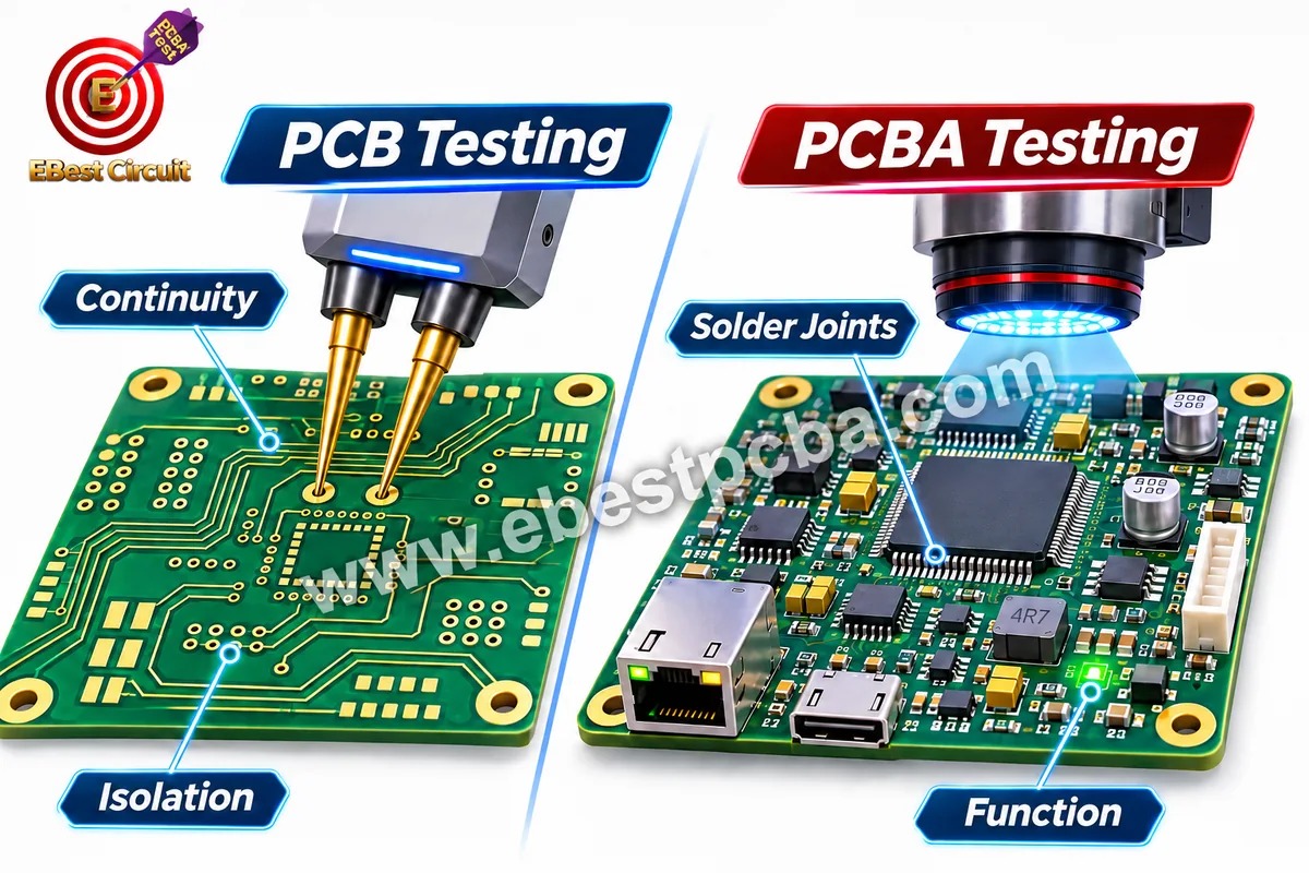
The key difference: A PCB electrical test confirms specified connections and isolation. It cannot determine whether the completed assembly will operate correctly.
For example, a bare PCB may pass its electrical test, while the finished PCBA fails because of an incorrectly installed component. This is why manufacturers inspect and test boards at multiple production stages.
What PCB Testing Methods Are Used Before Assembly?
Bare PCB testing primarily covers electrical connections, internal structures, board dimensions, and controlled impedance. Each method checks a different manufacturing requirement.
PCB Electrical Testing
PCB electrical testing verifies continuity between connected points and isolation between separate circuits.
- Continuity test: Identifies broken traces, open vias, and disconnected nets.
- Isolation test: Detects unintended connections and electrical shorts.
- Test reference: Uses the approved PCB netlist or equivalent electrical test data.
Electrical testing is a fundamental part of bare PCB inspection. However, a passing result does not establish how a marginal connection will perform after repeated temperature changes.
Flying Probe Testing
Flying probe testing uses movable probes to contact selected PCB test points without a dedicated test fixture.
- Best for: Prototypes and low-volume orders.
- Detects: Electrical opens and shorts.
- Main advantage: Flexible programming for PCB design revisions.
- Limitation: Testing can take longer on boards with many networks.
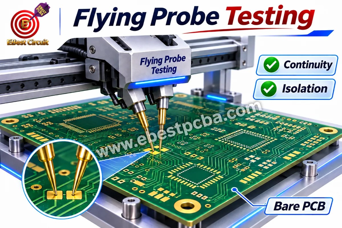
Flying probe testing is particularly useful when a PCB design is still changing because it avoids the cost of repeatedly modifying a dedicated fixture.
Fixture-Based Electrical Testing
Fixture-based electrical testing uses a customized arrangement of probes to test multiple points on a PCB.
- Best for: Stable designs and high-volume production.
- Detects: Electrical opens and shorts.
- Main advantage: Fast testing across repeated production batches.
- Limitation: Requires dedicated fixture development.
Once a PCB design is finalized, fixture-based testing can reduce the testing time per board.
Microsection Analysis
Microsection analysis examines a polished cross-section of a PCB to assess internal manufacturing quality.
It can reveal:
- Plated-through-hole copper thickness.
- Via plating voids and cracks.
- Inner-layer registration.
- Dielectric thickness.
- Laminate separation.
Since microsection analysis is destructive, manufacturers typically use selected samples or test coupons.
Controlled Impedance Testing
Controlled impedance testing measures the impedance of designated transmission-line structures, commonly using time-domain reflectometry (TDR).
It is important for:
- High-speed digital circuits.
- RF and microwave PCB designs.
- Differential signal routing.
- Impedance-controlled multilayer boards.
For example, a 100 Ω differential impedance requirement with a ±10% tolerance gives an acceptable measured range of 90–110 Ω.
How Do SPI, AOI, and X-Ray Inspection Detect Assembly Defects?
SPI, AOI, and X-ray inspection detect different assembly defects. SPI checks solder paste before component placement, AOI inspects visible assembly features, and X-ray examines hidden solder connections.
| Method | Inspection Stage | Main Defects Detected |
|---|---|---|
| SPI | After solder paste printing | Insufficient paste, excess paste, offset |
| AOI | After placement or soldering | Missing parts, polarity, visible solder defects |
| X-ray / AXI | After soldering | Hidden bridges, voids, BGA defects |
Solder Paste Inspection (SPI)
SPI measures solder paste deposits after stencil printing. A 3D SPI system can inspect paste height, area, volume, and alignment.
- Insufficient solder paste: May contribute to weak or incomplete joints.
- Excessive solder paste: Increases solder bridging risk.
- Paste misalignment: May affect component placement and soldering.
- Uneven deposits: Can contribute to inconsistent solder-joint formation.
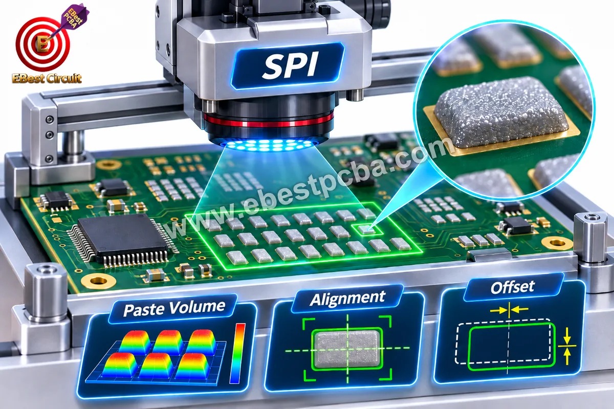
SPI helps detect printing problems before components are placed, reducing downstream rework.
Automated Optical Inspection (AOI)
AOI uses cameras and image-processing software to inspect visible PCB assembly features.
Common defects include:
- Missing components.
- Incorrect component orientation.
- Component misalignment.
- Visible solder bridges.
- Tombstoning.
- Insufficient or irregular visible solder joints.
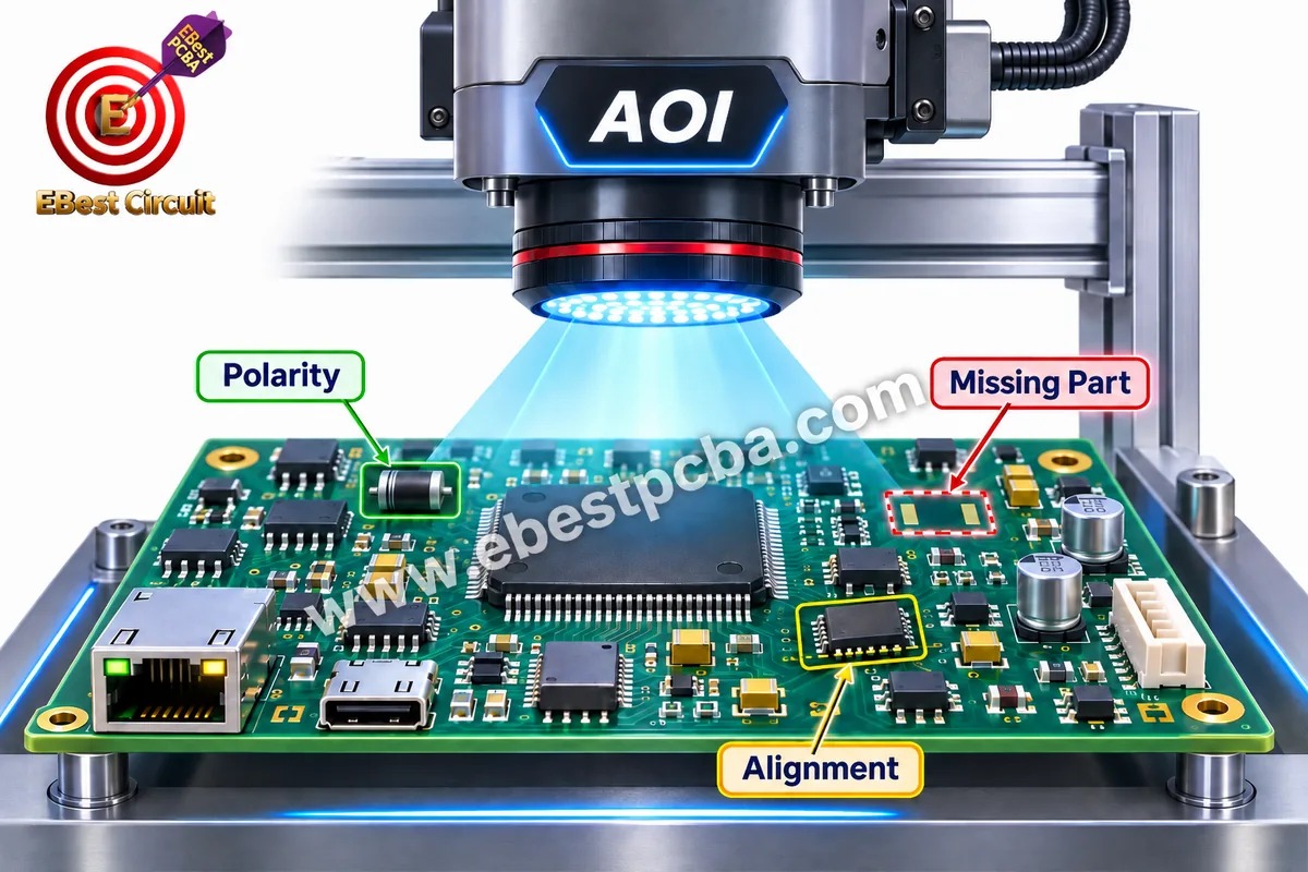
AOI works well for repeatable inspection, although hidden solder joints require other methods.
X-Ray Inspection and Automated X-Ray Inspection (AXI)
X-ray inspection examines solder connections that are difficult to see with optical inspection.
Typical applications include:
- BGA solder-ball inspection.
- QFN thermal pad inspection.
- Hidden solder bridges.
- Solder void assessment.
- Selected internal connection investigations.
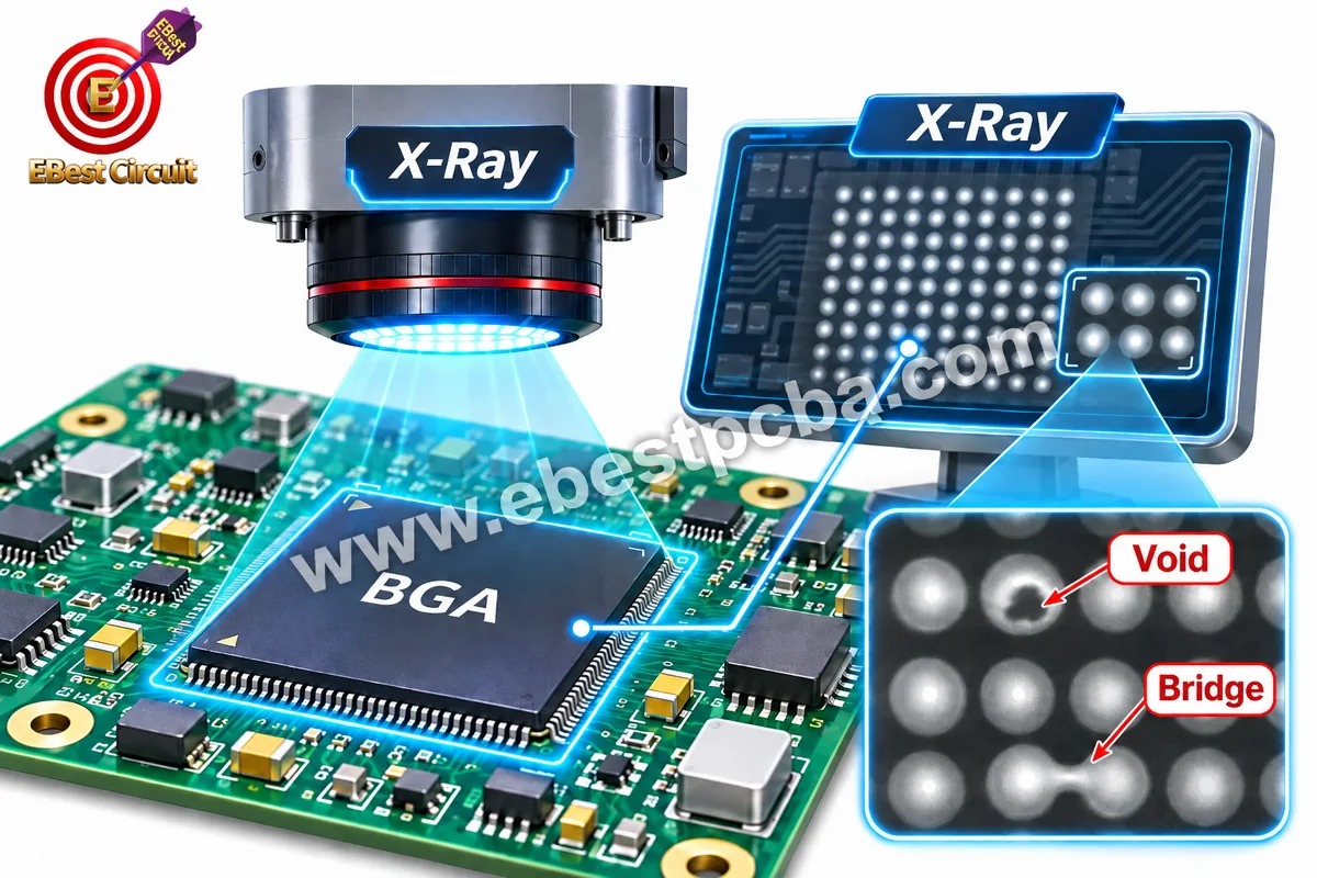
For BGA assemblies, X-ray provides valuable information about solder-ball geometry and voiding. Electrical testing may still be necessary to establish connection performance.
What Do ICT, Flying Probe, and Functional Testing Prove?
ICT and PCBA flying probe testing check selected electrical connections and component characteristics. Functional testing verifies whether the assembled circuit performs its intended tasks.
| Method | What It Checks | Best Application |
|---|---|---|
| ICT | Component values, opens, shorts | Repeat production |
| Flying Probe | Accessible electrical points | Prototypes and small batches |
| FCT | Defined circuit functions | Completed assemblies |
In-Circuit Testing (ICT)
ICT measures selected electrical characteristics of assembled components and their connections.
Depending on the design, it can identify:
- Incorrect resistor values.
- Missing components.
- Short circuits.
- Open connections.
- Certain component orientation errors.
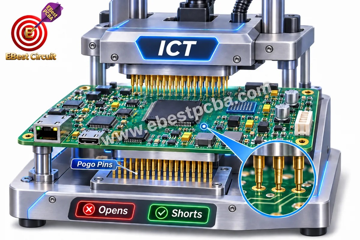
ICT is useful for locating assembly faults. Its coverage depends on test-point accessibility and circuit design.
PCBA Flying Probe Testing
Flying probe equipment can also test populated boards through accessible electrical points.
- Best for: Engineering samples and changing designs.
- Checks: Selected network connections and component measurements.
- Advantage: Minimal dedicated fixture requirements.
- Consideration: Test speed and coverage depend on accessibility.
When comparing flying probe testing vs ICT, consider test access, design stability, batch size and fixture investment. For low-volume orders, flying probe can provide useful electrical fault detection without dedicated ICT fixture tooling.
Functional Circuit Testing (FCT)
PCB functional testing (FCT) powers the completed assembly and checks its response against the product’s functional specifications.
Common tests include:
- Supply voltage and current measurement.
- Power-up and startup verification.
- Communication interface testing.
- Input and output signal checks.
- Sensor response and calibration.
- Firmware and control function verification.
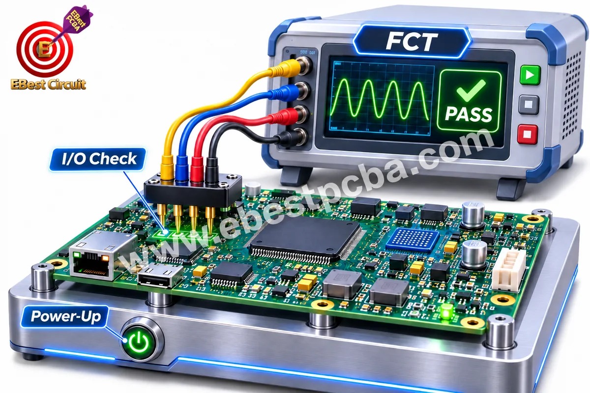
For example, a motor-control PCBA may pass FCT after its power supply, communication interface, and motor-drive outputs meet the programmed test limits.
A functional test confirms the behaviors covered by its test program. Additional testing may be necessary for environmental performance and long-term reliability.
When Is Boundary Scan Testing Useful for Complex PCBAs?
Boundary scan testing is useful when dense digital PCBAs have limited physical test-point access. It allows compatible integrated circuits to test selected interconnections through built-in test logic.
It is commonly used for:
- FPGA-based assemblies: Checking supported digital connections.
- Processor interfaces: Detecting certain interconnection faults.
- High-density BGA boards: Testing accessible digital networks without direct physical probing.
- Compatible programmable devices: Supporting selected programming and test operations.
Boundary scan follows the IEEE 1149.1 test access architecture. Its effectiveness depends on component compatibility, circuit design, and test-program coverage.
For complex assemblies, it can complement ICT and functional testing by improving access to selected digital interconnections.
Which PCB Reliability Tests Evaluate Long-Term Performance?
PCB reliability testing evaluates how boards and assemblies respond to temperature, humidity, vibration, and electrical stress. These tests help engineers assess specified failure mechanisms and support product qualification.
| Reliability Test | What It Evaluates |
|---|---|
| Thermal Cycling | Temperature-related fatigue |
| Thermal Shock | Rapid temperature transitions |
| Vibration Testing | Mechanical stress resistance |
| Humidity Testing | Moisture-related degradation |
| Insulation Resistance | Electrical leakage |
| Solderability Testing | Solder wetting behavior |
| Burn-In | Selected early-life failures |
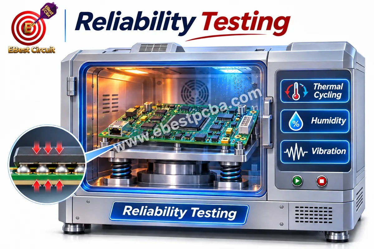
Thermal Cycling and Thermal Shock
Thermal cycling repeatedly exposes a PCB or PCBA to specified high and low temperatures.
It helps evaluate:
- Solder-joint fatigue.
- Plated-through-hole reliability.
- Material expansion mismatch.
- Interconnect integrity.
Thermal shock applies comparatively rapid temperature transitions to assess performance under sudden thermal changes.
Humidity and Insulation Resistance Testing
Humidity exposure can affect insulation performance and contribute to corrosion or electrical leakage.
Testing may include:
- Humidity exposure under controlled conditions.
- Surface insulation resistance measurements.
- Leakage-current monitoring.
- Post-exposure electrical verification.
These tests are relevant to electronics used in demanding environments.
Vibration Testing
Vibration testing evaluates an assembly’s response to specified mechanical loads.
It can reveal weaknesses in:
- Heavy component attachments.
- Connectors.
- Solder joints.
- Mechanical mounting structures.
Burn-In Testing
Burn-in operates electronic assemblies under defined electrical or thermal stress.
It is used to screen for selected early-life weaknesses before shipment. The test duration and conditions depend on product requirements.
Reliability test results apply to the tested samples and conditions. Qualification testing supports reliability assessment, while routine inspection helps control manufacturing consistency.
How Should Engineers Choose the Right PCB and PCBA Testing Strategy?
The best testing strategy matches the board’s design, production volume, and failure risks. More tests do not automatically produce better coverage when several methods inspect the same features.
| PCB or PCBA Type | Suggested Testing |
|---|---|
| Standard bare PCB | Visual inspection + E-test |
| HDI / multilayer PCB | E-test + microsection sampling |
| Controlled impedance PCB | E-test + impedance measurement |
| Prototype PCBA | SPI + AOI + targeted electrical/FCT |
| BGA assembly | SPI + AOI + X-ray + electrical testing |
| High-volume PCBA | SPI + AOI + ICT + FCT |
| High-reliability PCBA | Defined inspection + FCT + qualification testing |
Before finalizing a test plan, engineers should consider three factors:
- Defect risk: Identify critical circuits, hidden joints, fine-pitch components, and sensitive electrical connections.
- Test coverage: Determine which faults each method can detect and where coverage gaps remain.
- Production volume: Balance fixture costs, testing time, inspection requirements, and repeatability.
For example, flying probe testing may be appropriate for prototype batches, while a high-volume design may justify dedicated ICT fixtures.
The final test plan should define acceptance limits, test frequency, and required records before manufacturing begins.
What PCB Testing Standards and Reports Should Buyers Request?
PCBA testing standards define different aspects of workmanship, process requirements and test methods. Buyers should request testing against the applicable IPC standards, approved manufacturing specifications, and documented acceptance criteria. Test reports should clearly show what was inspected and whether the results passed.
| Standard | Application |
|---|---|
| IPC-A-600 | Bare PCB acceptability |
| IPC-6012 | Rigid PCB performance requirements |
| IPC-9252 | Bare PCB electrical testing |
| IPC-A-610 | Electronic assembly acceptability |
| IPC J-STD-001 | Soldered assembly requirements |
| IPC-TM-650 | Material and test methods |
| IEEE 1149.1 | Boundary scan testing |
| IPC-9701 | Solder attachment reliability |
The required standard revision and product acceptance class should be agreed upon during project qualification.
A useful PCB or PCBA test report should include:
- Board identification: Part number, revision, and production lot.
- Test method: Equipment and test-program identification.
- Acceptance limits: Applicable specifications and pass/fail criteria.
- Test results: Measured values or inspection outcomes.
- Traceability: Relevant board or batch identification.
- Failure records: Rework, corrective action, and retest information where applicable.
For medical, automotive, aerospace, and other controlled applications, additional customer-specific qualification and documentation requirements may apply.
How Does EBest PCBA Support PCB and PCBA Quality Control?
EBest PCBA supports PCB and PCBA quality control through coordinated fabrication, SMT assembly, process inspection, electrical testing, and manufacturing traceability. Our goal is to identify production defects at the appropriate stage and provide customers with clear manufacturing and testing support.
Our PCB Assembly and Testing Capabilities
| Capability | EBest PCBA |
|---|---|
| SMT Production | 4 lines: 2 JUKI + 2 YAMAHA |
| Component Size | Down to 01005 |
| BGA Pitch | Down to 0.2 mm |
| Solder Paste Inspection | 3D SPI |
| Optical Inspection | AOI |
| Hidden Joint Inspection | X-ray / AXI |
| In-Circuit Testing | ICT |
| Functional Testing | Project-specific FCT |
| Traceability | MES single-board tracking |
| Engineering Support | Free DFM |
| Minimum Order | No MOQ |
Why Customers Choose EBest PCBA
- Early Defect Detection: SPI, AOI, and X-ray inspection help identify soldering defects before final product delivery.
- Fine-Pitch Assembly Support: Four SMT lines support component placement down to 01005 and BGA pitch down to 0.2 mm.
- Electrical and Functional Verification: ICT and FCT capabilities support testing plans based on circuit design and customer requirements.
- Single-Board Traceability: MES records help connect manufacturing information with individual boards for quality investigations.
- Dedicated Engineering Support: One sales representative and three engineers coordinate manufacturing questions throughout the project.
- Flexible Production: No MOQ and free DFM support help customers move from prototype validation to repeat orders.
Our quality management certifications include ISO 9001, ISO 13485, IATF 16949, and AS9100D, supporting supplier qualification for different industries.
Need PCB manufacturing and assembly with a clear testing plan? EBest PCBA offers coordinated fabrication, component sourcing, SMT assembly, inspection, and testing. Send your Gerber files, BOM, quantities, and testing requirements to sales@ebestpcba.com for a free DFM review, quotation, and delivery schedule confirmation.
FAQs about PCB and PCBA Testing Methods
What is the most common PCB testing method?
Electrical continuity and isolation testing is a common method for bare PCBs. It detects opens and shorts by checking connections against the approved electrical test data.
What is the difference between AOI and X-ray inspection?
AOI checks visible components and solder joints, while X-ray examines hidden solder connections beneath packages such as BGA and QFN.
Is flying probe testing better than ICT?
Flying probe testing is generally more flexible for prototypes and small batches. ICT is often faster for stable, high-volume PCBA production where dedicated test fixtures are justified.
Can a PCBA pass AOI but fail functional testing?
Yes. AOI checks visible assembly features, while functional testing verifies electrical operation. Incorrect component values, internal failures, or firmware problems may cause a board to fail FCT even after passing AOI.
Does X-ray inspection detect every BGA solder defect?
No. X-ray can reveal many hidden solder defects, including bridges and voids. Some connection defects require additional inspection techniques or electrical verification.
What is the difference between ICT and FCT?
ICT checks selected component values and electrical connections. FCT powers the board and verifies defined circuit functions under specified test conditions.
Are reliability tests performed on every PCB?
Usually not. Destructive and environmental reliability tests commonly use qualification samples or defined sampling plans. Routine electrical tests and non-destructive inspections may be applied to individual production boards.
What testing information should I provide to a PCBA manufacturer?
Provide the PCB design files, BOM, assembly drawings, electrical requirements, test procedures, acceptance limits, and any required fixtures or firmware. This allows the manufacturer to review test coverage and prepare an appropriate quotation.
How Can We Define a Testing Plan for Your Next Build?
PCB and PCBA testing methods verify different aspects of manufacturing quality, from bare-board electrical integrity to solder-joint inspection and completed circuit performance. Combining suitable electrical, optical, X-ray, functional, and reliability tests helps detect defects at the right stage and improve production consistency. At EBest PCBA, our SMT manufacturing capabilities, SPI, AOI, X-ray, ICT, FCT, and MES traceability support customer-specific quality requirements from prototypes to repeat production. Contact sales@ebestpcba.com to discuss your PCB fabrication, assembly, and testing needs.